Poly-crystalline thin film transistor and fabrication method thereof

Inactive Publication Date: 2006-03-07
LG DISPLAY CO LTD
View PDF10 Cites 1 Cited by
  • Summary
  • Abstract
  • Description
  • Claims
  • Application Information

AI Technical Summary

Benefits of technology

[0010]Therefore, an object of the present invention is to provide a low current

Problems solved by technology

However, since the mobility of a-Si thin film transistors is low, such transistors are not well suited for LCD drive applications.
However, poly-crystalline silicon thin film transistors constructed as shown in FIG. 1 tend to have

Method used


Image

  • Poly-crystalline thin film transistor and fabrication method thereof
  • Poly-crystalline thin film transistor and fabrication method thereof
  • Poly-crystalline thin film transistor and fabrication method thereof

Examples


Example

[0019]Reference will now be made in detail to the illustrated embodiments of the present invention, examples of which are shown in the accompanying drawings.

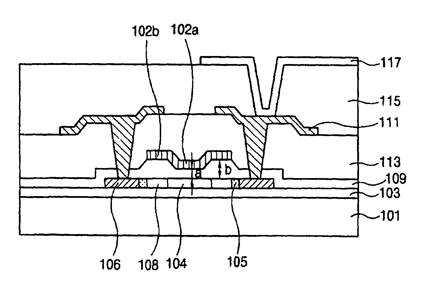
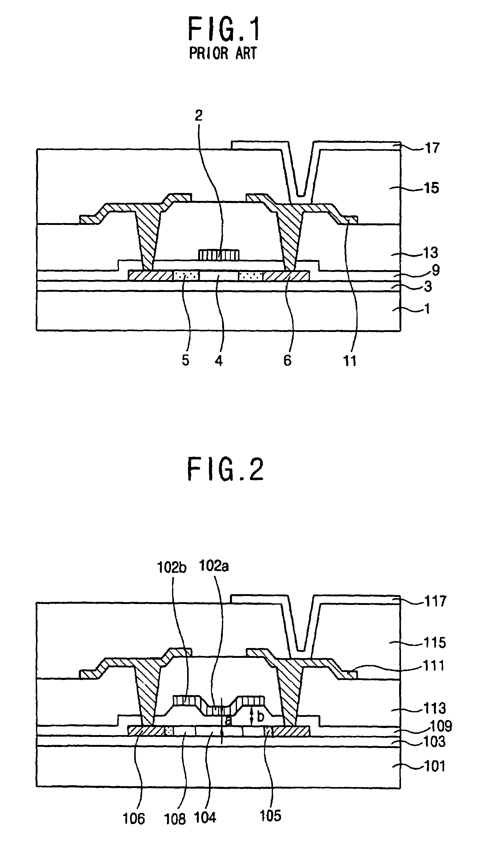
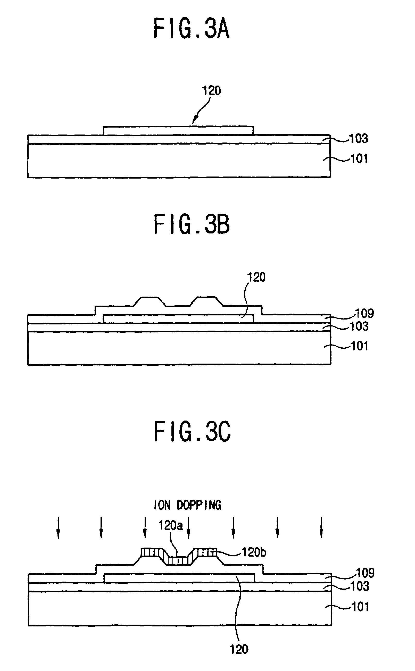
[0020]The principles of the present invention provide for poly-crystalline silicon thin film transistors having low leakage current and high ON-state current. Such transistors are adaptable for use in liquid crystal displays. According to the principles of the present invention, such a poly-crystalline silicon thin film transistor includes a gate electrode that is comprised of a main gate electrode and of auxiliary gate electrodes that extend from the main gate. In addition, the transistor includes a poly-crystalline silicon layer comprised of a channel layer below the main gate electrode, offset regions below the auxiliary gate electrodes, sequentially doped regions along sides of the offset regions, and source and drain regions along sides of the sequentially doped regions.

[0021]The principles of the present invention provide ...


PUM


Abstract

A thin film transistor and its fabrication method. The transistor includes a buffer layer on a substrate, and a poly-crystalline semiconductor layer on the buffer layer. The poly-crystalline semiconductor layer includes a channel layer, offset regions along sides of the channel layer, sequential doping regions along sides of the offset regions, and source and drain regions. The doping concentration is sequentially changed in the sequential doping region. A sloped gate insulation layer is on the poly-crystalline semiconductor layer. A gate electrode having a main gate electrode and auxiliary gate electrodes is on the sloped insulation layer. An interlayer is over the gate electrode and source and drain electrodes are formed in contact with the source and drain regions and on the interlayer. The poly-crystalline semiconductor layer is formed by ion doping a poly-crystalline semiconductor layer through the gate insulation layer while using the gate electrode as a mask.

Description

[0001]This application is a Divisional of prior U.S. application Ser. No. 10 / 279,934, filed Oct. 25, 2002 now U.S. Pat No. 6,713,825.BACKGROUND OF THE INVENTION[0002]1. Field of the Invention[0003]The present invention relates to poly-crystalline thin film transistors and to their fabrication. More particularly, the present invention relates to poly-crystalline thin film transistors having multiple section gate electrodes and multiple section semiconductor layers.[0004]2. Description of the Background Art[0005]Thin film transistors used in active matrix liquid crystal displays are typically made of amorphous silicon (a-Si). Amorphous silicon is advantageous in that it enables large area displays that can be fabricated at low temperature on low-cost glass substrates. However, since the mobility of a-Si thin film transistors is low, such transistors are not well suited for LCD drive applications. In contrast, poly-crystalline silicon thin film transistors have high mobility. This make...

Claims


Application Information

Patent Timeline
IPC IPC(8): H01L21/00H01L21/84G02F1/136H01L21/336H01L29/423H01L29/49H01L29/786
CPCH01L29/42384H01L29/4908H01L29/78621H01L29/66757H01L2029/7863G02F1/136
Inventor HWANG, HAN-WOOK
Owner LG DISPLAY CO LTD
Why Eureka
Try Eureka