Voltage detecting circuit

Inactive Publication Date: 2005-02-22
ABLIC INC
View PDF10 Cites 1 Cited by
  • Summary
  • Abstract
  • Description
  • Claims
  • Application Information

AI Technical Summary

Benefits of technology

According to a third aspect of the present invention, in the second aspect of the invention, there is provided a voltage detecting circuit, in which both an absolute value of the threshold voltage of the second conductivity type enhancement MIS transistor connected to the second constant current circuit is higher than absolute values of threshold voltages of the second conductivity type enhancement MIS transistors constituting the current mirror circuit and the amplifying circuit. Thus, it becomes possible to reduce a leak current of the circuit to thereby lower a consumed electric current.
According to a fourth aspect of the present invention, there is provided a voltage detecting circuit including: a current mirror circuit having at least one input terminal and at least one output terminal; a first constant current circuit with an output terminal connected to the input terminal of the current mirror circuit; a first conductivity type enhancement MIS transistor having a gate electrode, a drain electrode, and a source electrode, the drain electrode being connected to the output terminal of the current mirror circuit, and the source electrode being connected to a first power supply potential; a second constant current circuit with an output terminal connected to the gate electrode of the first conductivity type MIS transistor; a second conductivity type enhancement MIS transistor having a first threshold voltage and including a gate electrode, a drain electrode, and a source electrode, the drain electrode being connected to the output terminal of the second constant current circuit, the source electrode being connected to a second power supply potential, and the gate electrode being connected to the first power supply potential; a second conductivity type enhancement MIS transistor having a second threshold voltage and including a gate electrode, a drain electrode, and a source electrode, the drain electrode being connected to the output terminal of the second constant current circuit, and the source electrode being connected to the second power supply potential; an inverter circuit including an output terminal and an input terminal, the output terminal being connected to the gate electrode of the second conductivity type enhancement MIS transistor having the second threshold voltage; and an amplifying circuit including at least one input terminal and at least one output terminal, the input terminal being connected to the output terminal of the current mirror circuit, the output terminal being connected to an input of the inverter circuit, and the output terminal being a terminal for outputting a voltage detection output of the power supply potential. Thus, it becomes possible to reduce a leak current of the circuit to thereby lower a consumed electric current.
According to a fifth aspect of the present invention, in the fourth aspect of the invention, there is provided a voltage detecting circuit, in which the current mirror circuit includes a second conductivity type first MIS transistor and a second conductivity type second MIS transistor, a source electrode of the second conductivity type first MIS transistor is connected to the second power supply potential, a gate electrode and a drain electrode are connected in common and are connected to an input terminal of the current mirror circuit, a source electrode of the second conductivity type second MIS transistor is connected to the second power supply potential, a drain electrode is connected to the output terminal of the current mirror circuit, a gate electrode is connected to the gate electrode and the drain electrode of the second conductivity type first MIS transistor, the first constant current circuit includes a first conductivity type depletion MIS transistor, a source electrode and a gate electrode of the first conductivity type depletion MIS transistor constituting the first constant current circuit is connected to the first power supply potential, a drain electrode is connected to the output terminal of the first constant current circuit, the second constant current circuit includes a first conductivity type depletion MIS transistor, a source electrode and a gate electrode of the first conductivity type depletion MIS transistor constituting the second constant current circuit are connected to the first power supply potential, a drain electrode is connected to the output terminal of the second constant current circuit, and the amplifying circuit is an inverter circuit including a first conductivity type enhancement MIS transistor and a second conductivity type enhancement MIS transistor. Thus, it becomes possible to reduce a leak current of the circuit to thereby lower a consumed electric current.
According to a sixth aspect of the present invention, in the fifth aspect of the invention, there is provided a voltage detecting circuit, in which both an absolute value of the threshold voltage of the second conductivity type enhancement MIS transistor having the first threshold voltage and connected to the second constant circuit and an absolute value of the threshold

Problems solved by technology

This is because immediately after detection release of the potential at the node N2, the gate electrode of the N-type enhancement MIS transistor 2004 can not be sufficiently biased, and the current drive capability of the N-type enhancement MIS transistor 2004 can not sufficiently overcome the current supply capability of the current mir

Method used


Image

  • Voltage detecting circuit
  • Voltage detecting circuit
  • Voltage detecting circuit

Examples


embodiment 1

(Embodiment 1)

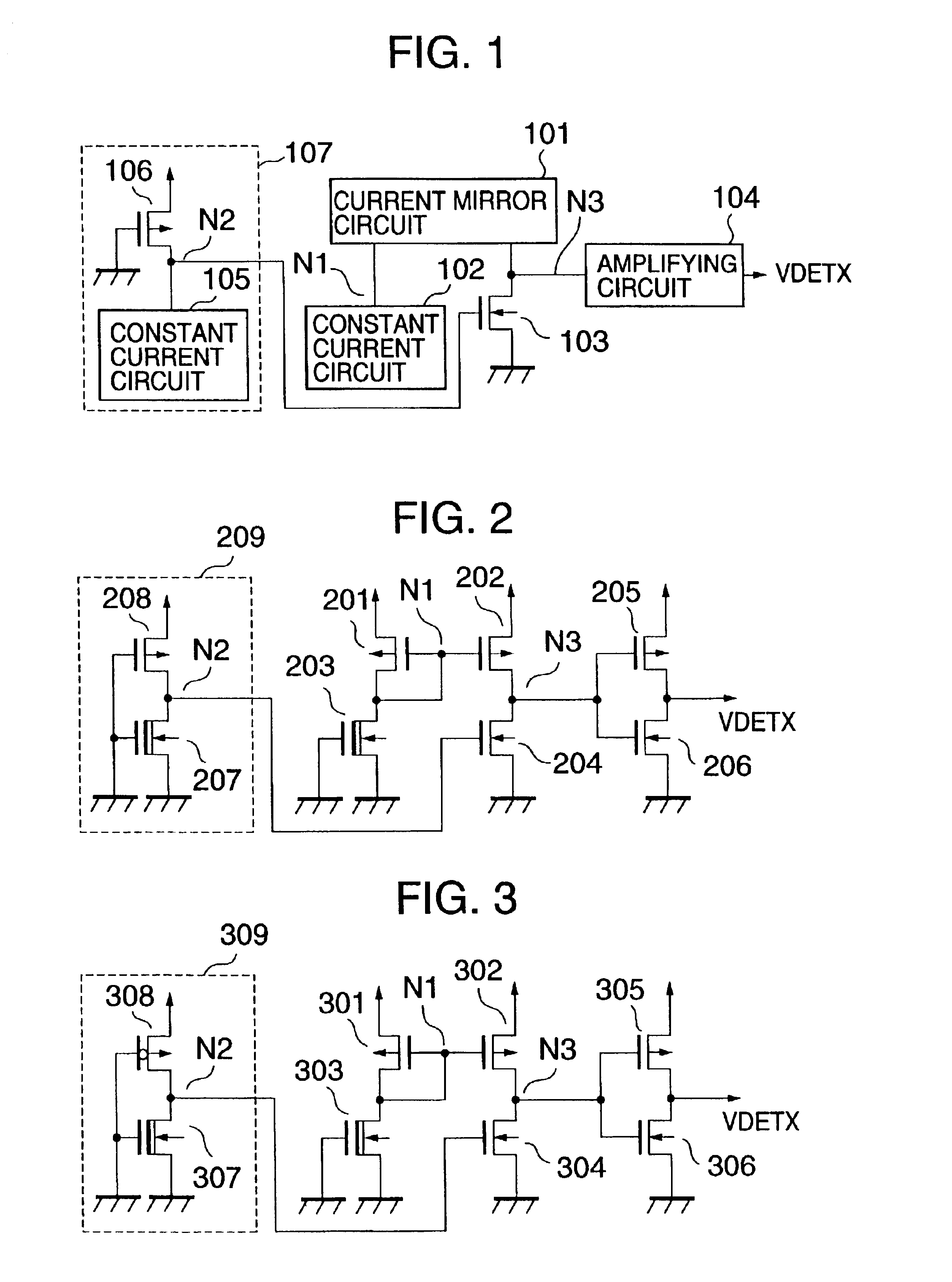
FIG. 1 is a block diagram showing a structure of a voltage detecting circuit according to Embodiment 1 of the invention.

In the present invention, a first constant current circuit 102 is connected to an input side N1 of a current mirror circuit 101, an N-type enhancement MIS transistor 103 is connected to an output side N3, an amplifying circuit 104 is connected to the output side N3 of the current mirror circuit, and the amplifying circuit outputs a detection output VDETX.

A gate of the N-type enhancement MIS transistor 103 is biased at a connection point N2 between a second constant current circuit 105 and a drain of a P-type enhancement MIS transistor 106. The second constant current circuit 105 and the P-type enhancement MIS transistor 106 constitute a bias circuit 107.

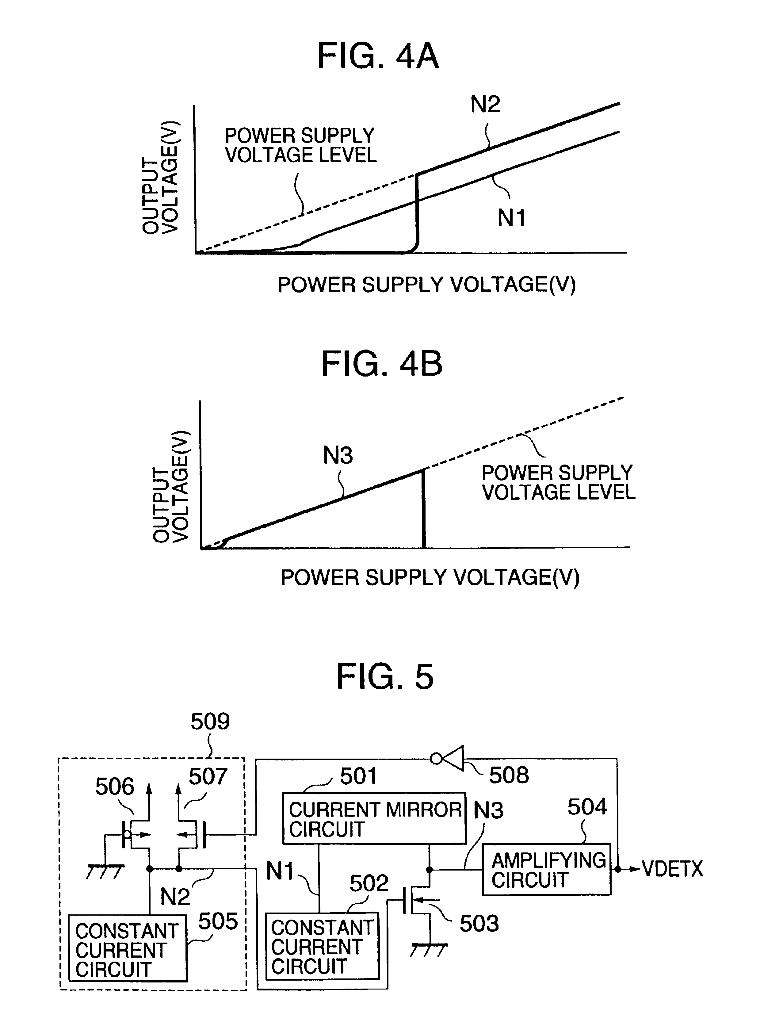
Since a gate of the P-type enhancement MIS transistor 106 is connected to ground as a first power supply potential, and its source is connected to Vcc as a second power supply voltage, a gate source vo...

embodiment 2

(Embodiment 2)

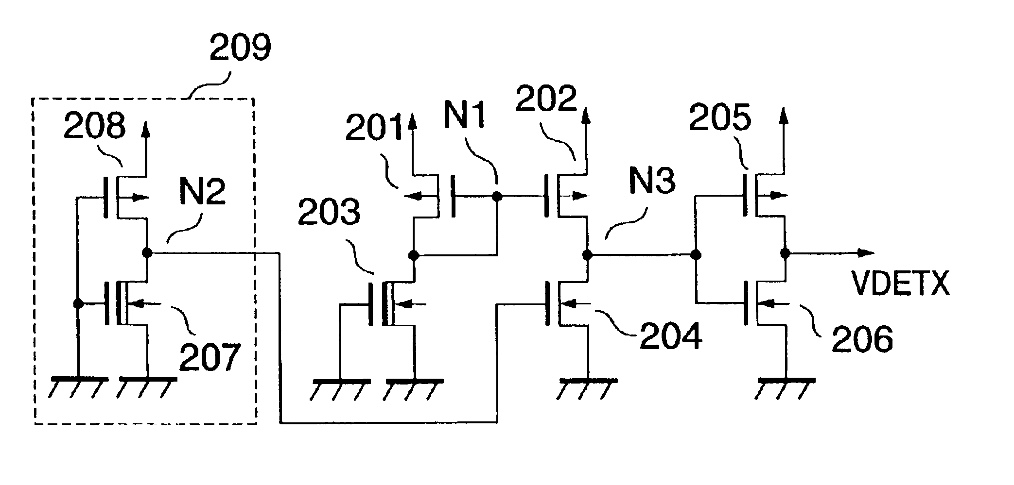
FIG. 2 is a circuit diagram showing a structure of a voltage detecting circuit according to Embodiment 2 of the present invention. In the figure, there is shown an example of a detailed structure of the current mirror circuit, the amplifying circuit and the constant current circuit of Embodiment 1.

A current mirror circuit is constituted by P-type enhancement MIS transistors 201 and 202 in which gates are connected in common, and the gate and drain of the P-type enhancement MIS transistor 201 are connected in common and serve as an input terminal N1 of the current mirror circuit.

A drain of the P-type enhancement MIS transistor 202 serves as an output terminal N3 of the current mirror circuit.

A P-type enhancement MIS transistor 208 and an N-type depletion MIS transistor 207 constitute a bias circuit 209.

Both the N-type depletion MIS transistors 203 and 207 operate as constant current elements in each of which a gate electrode and a source electrode are connected to groun...

embodiment 3

(Embodiment 3)

FIG. 3 is a circuit diagram showing a structure of a voltage detecting circuit according to Embodiment 3 of the present invention. In Embodiment 3, in order to obtain a relatively high detection voltage with high precision, a threshold voltage of a P-type enhancement MIS transistor 308 has a value higher than threshold voltages of P-type MIS transistors 301 and 302 constituting a current mirror circuit and a P-type MIS transistor 305 constituting an amplifying inverter. The intensities of the threshold voltages stated here are compared with each other in the absolute value.

A P-type enhancement MIS transistor 308 and an N-type depletion MIS transistor 307 constitute a bias circuit 309.

For example, threshold voltages of the P-type MIS transistors 301, 302 and 305 are made approximately −0.7 V, and that of the P-type MIS transistor 308 is made approximately −1.9 V.

As a result, approximately 1.9 V can be obtained as the detection voltage of the voltage detecting circuit of...


PUM


Abstract

There is provided a voltage detecting circuit in which a consumed electric current is small, accuracy is high, and an erroneous operation seldom occurs. In the voltage detecting circuit constituted by a bias circuit, a current mirror circuit, a load MIS transistor connected to the current mirror circuit in which current drive capability is changed by an output voltage of the bias circuit, and an amplifying inverter circuit, a potential change at an output node of the current mirror circuit at the time of detection and release of a power supply voltage is steeply changed, so that a leak current of the whole circuit can be decreased and a consumed electric current can be reduced. Besides, plural load P type MIS transistors of the bias circuit are prepared, so that a detection voltage and a release voltage can be made to have hysteresis, abnormal oscillation of a detection output VDETX in the vicinity of the detection and release voltage can be prevented, and an erroneous operation of a logic circuit to which the detection output is applied can be prevented.

Description

BACKGROUND OF THE INVENTION1. Field of the InventionThe present invention relates to a power supply voltage detecting circuit constituted by MIS transistors.2. Description of the Related ArtUp to now, in the case where a power supply voltage supplied in a semiconductor integrated circuit is low and a circuit operation is apt to become unstable, a circuit has been reset at the time of a low power supply voltage by using a power supply voltage detecting circuit as shown in FIG. 10.Hereinafter, the circuit will be described on the basis of the drawings.An N-type depletion MIS transistor 2003 in which a gate electrode and a source electrode are connected to ground and which operates as a constant current element, is connected to an input side of a current mirror circuit constituted by a P-type enhancement MIS transistor 2001 and a P-type enhancement MIS transistor 2002, and an N-type enhancement MIS transistor 2004 is connected to an output side node N3 of the current mirror circuit.Bes...

Claims


Application Information

Patent Timeline
IPC IPC(8): G01R19/165G05F1/10G05F3/26H03K17/30
CPCG01R19/16552G01R19/16519
Inventor MIYAGI, MASANORI
Owner ABLIC INC
Why Eureka
Try Eureka