Defect check method and device thereof

a technology of defect detection and detection method, applied in the field of check or inspection, can solve problems such as inability to detect defects, lower sensitivity, and false information

Inactive Publication Date: 2011-07-28
HITACHI HIGH-TECH CORP
View PDF3 Cites 23 Cited by
  • Summary
  • Abstract
  • Description
  • Claims
  • Application Information

AI Technical Summary

Benefits of technology

[0015]According to the present invention, it is possible to detect the kind of def

Problems solved by technology

However, inherently this should not be detected as the defect.
Thus, it is erroneous information.
However, this lowers the sensitivity, i.e., it is impossible to detect the defect having the difference value being equal to or less than that.
Further, determining the threshold value depending on the brightness for each local area brings about complicatedness or troublesome in an operation, and therefore this is not desirable for a user.
Also as a factor of hampering the sensitivity is a difference of brightness between the chops, caused due to variation of thickness of the patterns.
In the conventional comparison check with using the brightness, if there is such variation of the brightness, it

Method used


Image

  • Defect check method and device thereof
  • Defect check method and device thereof
  • Defect check method and device thereof

Examples


Embodiment Construction

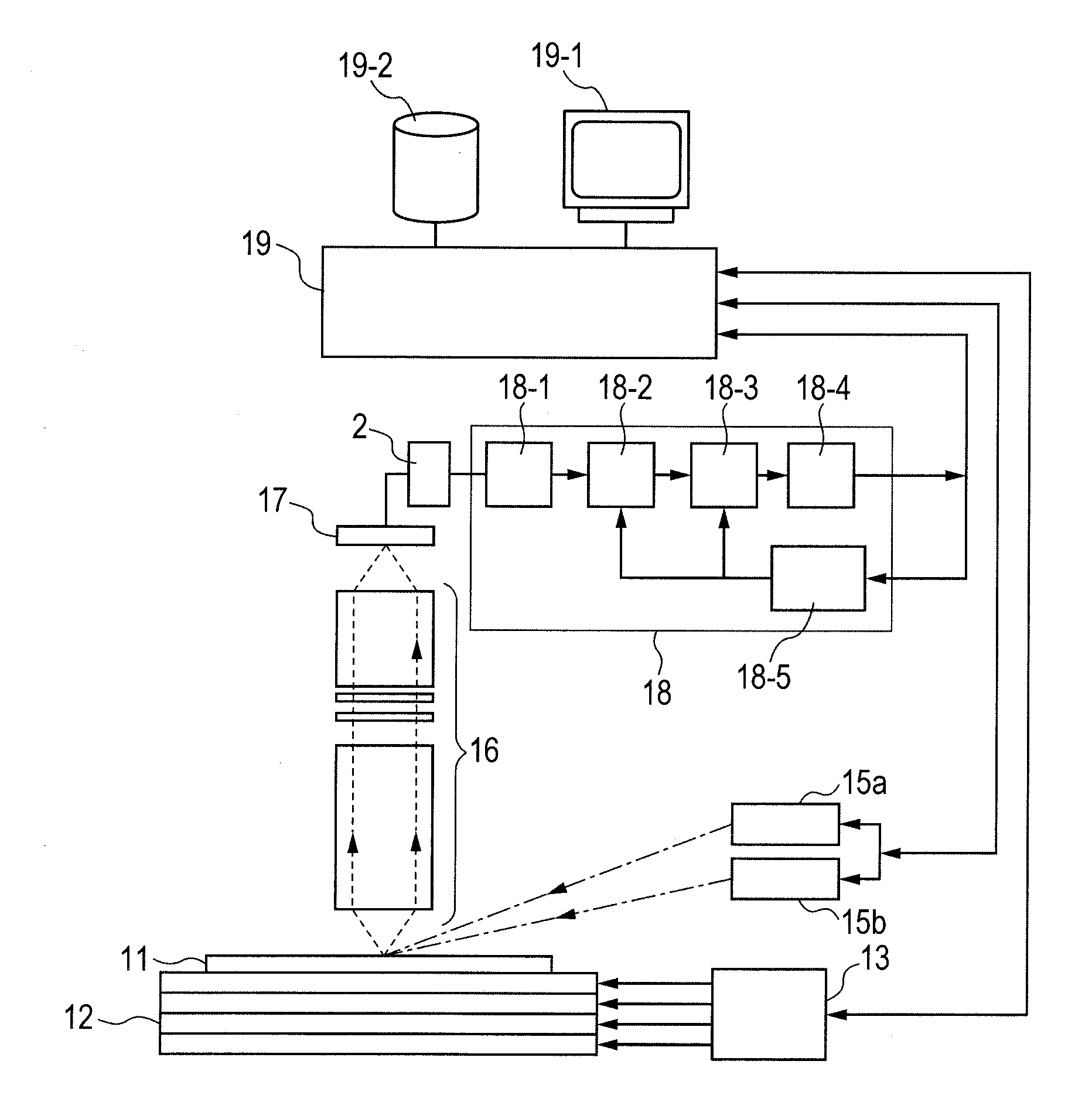
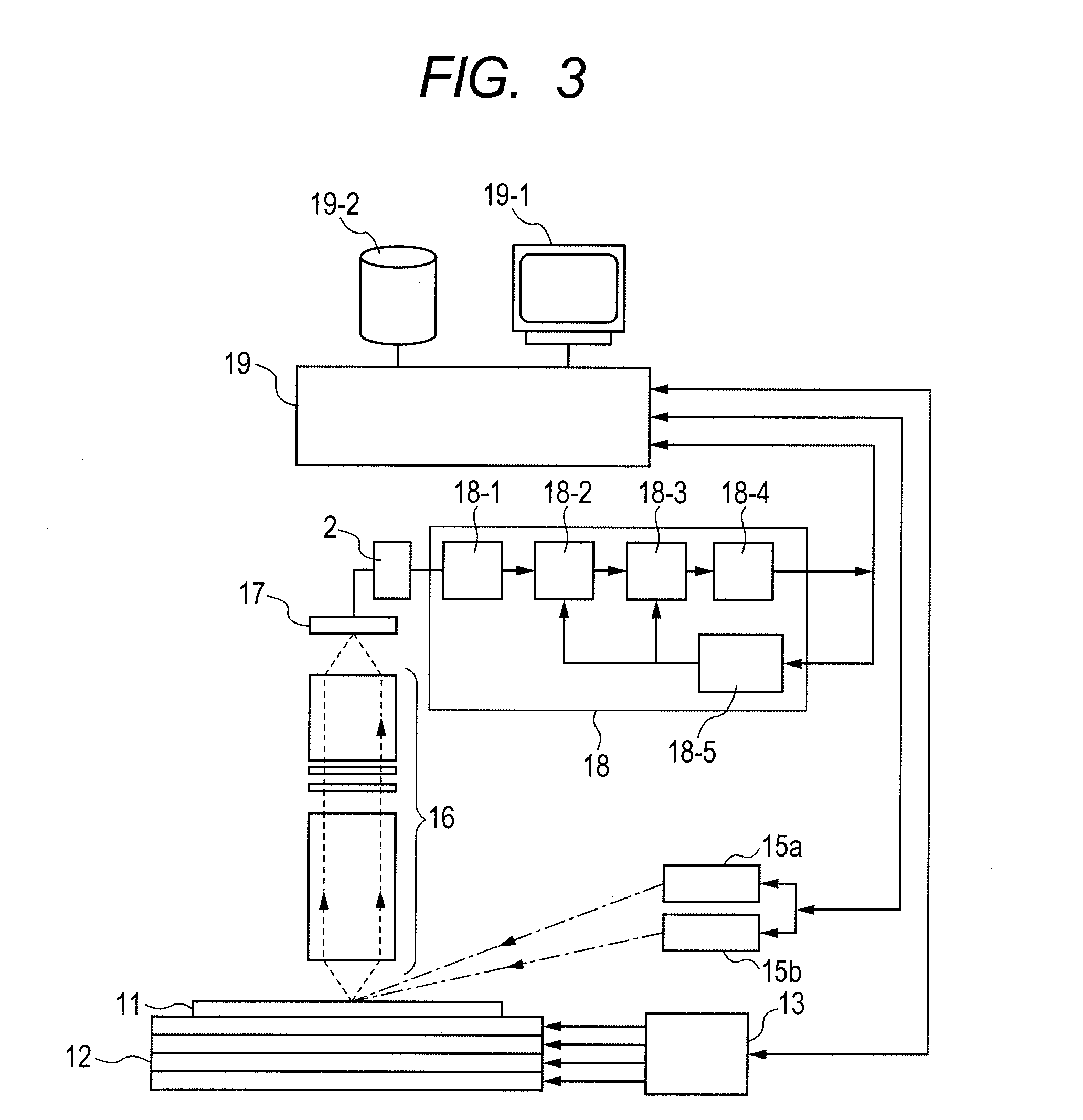
[0085]Hereinafter, an embodiment according to the present invention will be fully explained by referring to FIG. 1 through FIG. 17 attached herewith, showing an example of a defect check apparatus with a dark-field illumination targeting on a semiconductor wafer as an object to be inspected.

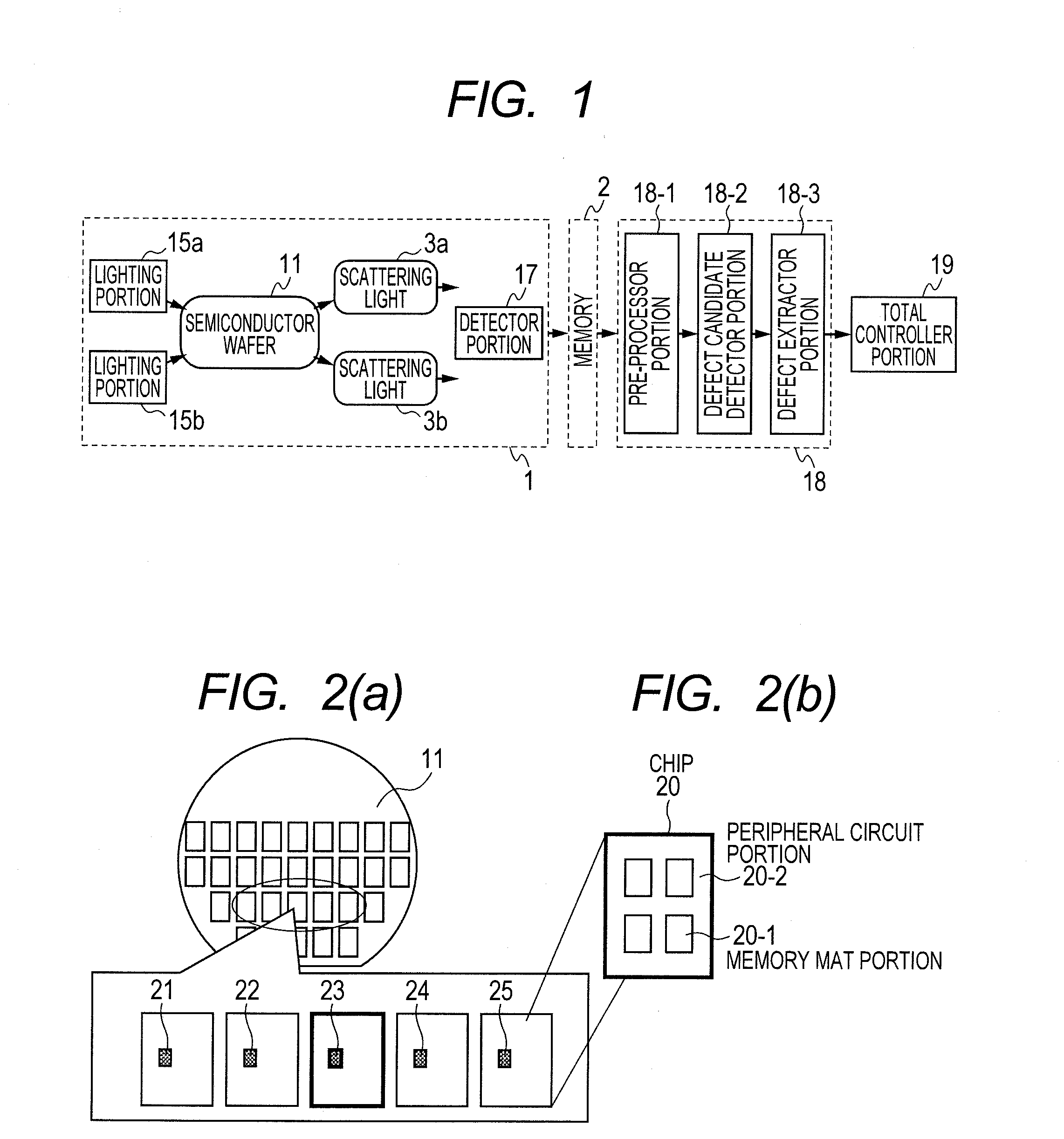
[0086]FIG. 1 is a diagram for showing the structures of the defect check apparatus according to the present invention. An optic portion 1 is so constructed as to have plural numbers of lighting portions 15a and 15b and a detector portion 17. The lighting portions 15a and 15b irradiate illumination lights, each having an optic condition different from each other, upon an object to be inspected (e.g., a semiconductor wafer 11) respectively. Due to the illumination lights by means of the lighting portion 15a and 15b, scattering lights are generated, respectively, and are detected in the form of a scattering-light intensity signal by means of the detector portion 17. The scattering-light intensity si...


PUM


Abstract

A defect inspection method for inspecting a defect(s) on an object to be inspected, within a step for determining parameter includes: a step for extracting a defect candidate on the object to be inspected with using said discriminant function with determining an arbitrary parameter; and a step for automatically renewing the parameter of said discriminant function, upon basis of teaching of defect information relating to the defect candidate, which is extracted in the step for extracting the defect candidate.

Description

TECHNICAL FIELD[0001]The present invention relates to a check or inspection for detecting a minute pattern defect and / or a foreign substance upon basis of a result of comparison, while comparing an image of an object to be inspected (i.e., a check image), which is obtained with using a light, a laser or an electron beam, etc., with a reference image, and in particular, it relates to a defect check or inspection method and a device thereof being suitable for conducting a visual inspection upon a semiconductor wafer, a TFT and / or photo mask and so on.BACKGROUND OF THE INVENTION[0002]As the conventional technology for conducting a defect detection with comparison between a detection image and a reference image is already known a method, which is described in a Patent Document 1. In this, an image of an object to be inspected, on which patterns are aligned repeatedly, is taken by a line sensor, sequentially, to be compared with an image delayed by an amount of a repetitive pattern pitch...

Claims


Application Information

Patent Timeline
IPC IPC(8): G06K9/00
CPCG01N21/956G01R31/311G06T2207/30148G06T2207/30121G06T7/001
Inventor SAKAI, KAORUMAEDA, SHUNJI
Owner HITACHI HIGH-TECH CORP
Why Eureka
Try Eureka