Electronic device and method of manufacturing the same

a technology of electronic devices and manufacturing methods, applied in the direction of cable junctions, cables/solid-state device details, cable terminations, etc., can solve the problems of low mechanical strength of metal joining, not finding pb-free solder which can be used in such high temperature, etc., and achieve the effect of improving the strength of metal conductors

Active Publication Date: 2011-08-11
DENSO CORP
View PDF4 Cites 20 Cited by
  • Summary
  • Abstract
  • Description
  • Claims
  • Application Information

AI Technical Summary

Benefits of technology

[0013]In view of the foregoing problems, it is an object of the present invention to effectively improve the strength of a metal conductor, in an electronic device in which an electronic component is mechanically joined with a joining member via the metal conductor made of porous noble metal.
[0014]According to an aspect of the present invention, an electronic device includes an electronic component, a joining member to be mechanically joined with the electronic component, and a metal conductor arranged between the electronic component and the joining member to mechanically join the electronic component and the joining member. The metal conductor is made of porous noble metal to have pores, and includes an end surface without being covered by the electronic component and the joining member. Furthermore, a reinforcing resin is impregnated from the end surface of the metal conductor to an inside of the metal conductor, to mechanically reinforce the metal conductor. Thus, the strength of the metal conductor can be effectively increased.
[0016]Thus, the reinforcing resin can be stably held in the metal conductor, thereby suitably improving the mechanical strength of the metal conductor. Furthermore, the primer is arranged at least between the end surface of the metal conductor and the mold resin to increase an adhesiveness therebetween, and the reinforcing resin is made of a resin material having a higher adhesion strength with the primer than the metal conductor. Therefore, adhesiveness between the primer and the metal conductor can be increased via the reinforcing resin. In addition, because the mold resin is configured to seal the electronic component, the joining member and the end surface of the metal conductor, the position of the metal conductor can be accurately maintained while restricting a bending or a shift of the metal conductor.
[0021]According to another aspect of the present invention, a method of manufacturing an electronic device includes of a step of mechanically joining an electronic component and a joining member via a metal conductor made of a porous noble metal such that the metal conductor has an end surface without being covered by the electronic component and the joining member, a step of applying a paste made of a resin material and a diluent for diluting the resin material, and a step of decompressing a space around the metal conductor to a pressure lower than an atmosphere pressure and lower than a vapor pressure of the diluent to evaporate and remove the diluent in the pores while introducing the paste into the pores of the metal conductor, so as to impregnate the resin material from the end surface of the metal conductor into the pores within the metal conductor. Furthermore, the decompressing is performed such that an inside of the metal conductor inside of the resin material is sealed by the resin material, and the inside of the metal conductor inside of the resin material has a pressure lower than a pressure outside of the metal conductor so as to apply a compression force from the outside of the metal conductor to the inside of the metal conductor. Thus, the diluents in the pores can be effectively evaporated and removed, thereby increasing the strength of the metal conductor.

Problems solved by technology

The electronic component may be used in a high temperature equal to or higher than 200° C. However, Pb-free solder which can be used in such high temperature has not been found, at the present time.
However, when the porous metal conductor is used for the metal joining, the mechanical strength of the metal joining is relatively low because the contact surfaces between the metal particles are small in the metal joining.

Method used


Image

  • Electronic device and method of manufacturing the same
  • Electronic device and method of manufacturing the same
  • Electronic device and method of manufacturing the same

Examples


first embodiment

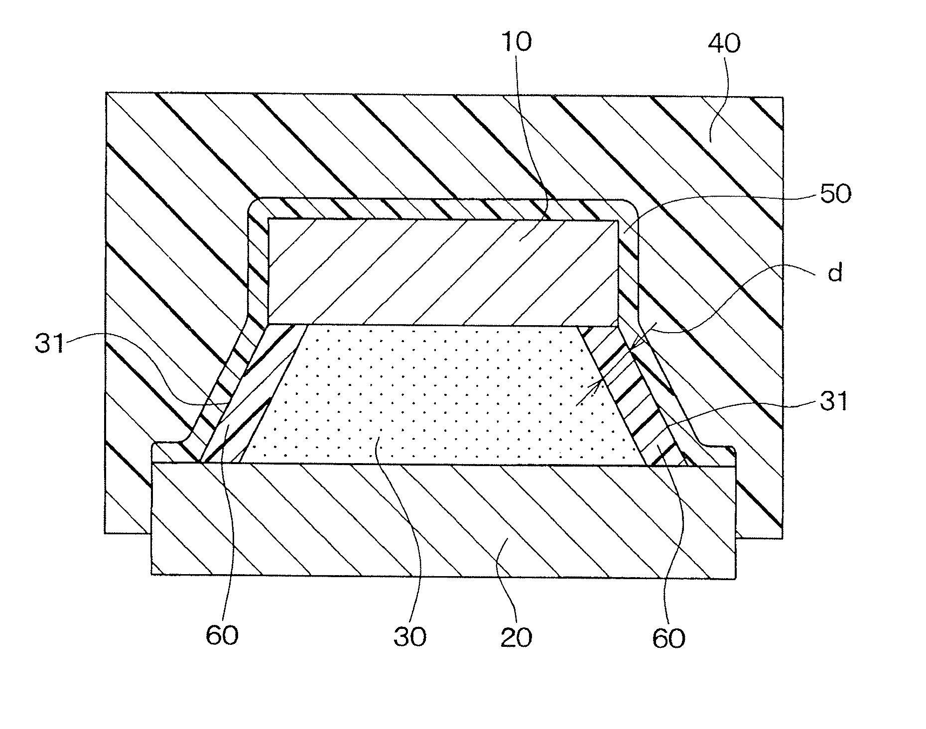
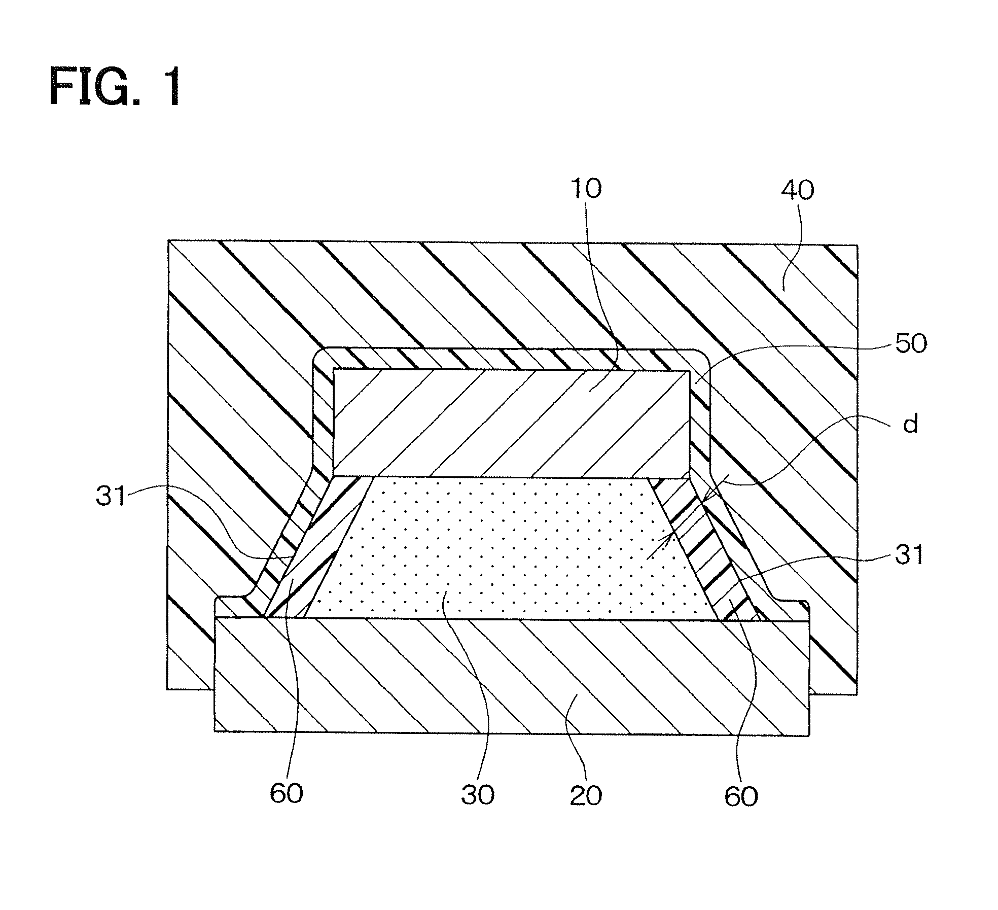
[0035]FIG. 1 is a schematic sectional view showing an electronic device according to a first embodiment of the present invention. In the first embodiment, the electronic device includes an electronic component 10, a member 20 to be joined (joining member), a metal conductor 30 configured to mechanically join the electronic component 10 and the joining member 20, and a mold resin 40 configured to seal the electronic component 10, the joining member 20 and the metal conductor 30.

[0036]The electronic component 10 may be any electronic part which radiates a large amount of heat when being driven. For example, the electronic component 10 may be an IC chip which has a large-scale integrated circuit, a power element such as a power transistor, etc.

[0037]The joining member 20 does not limit a special member. The joining member 20 may be any member to be joined mechanically with the electronic component 10. For example, the joining member 20 mechanically joined with the electronic component ...

second embodiment

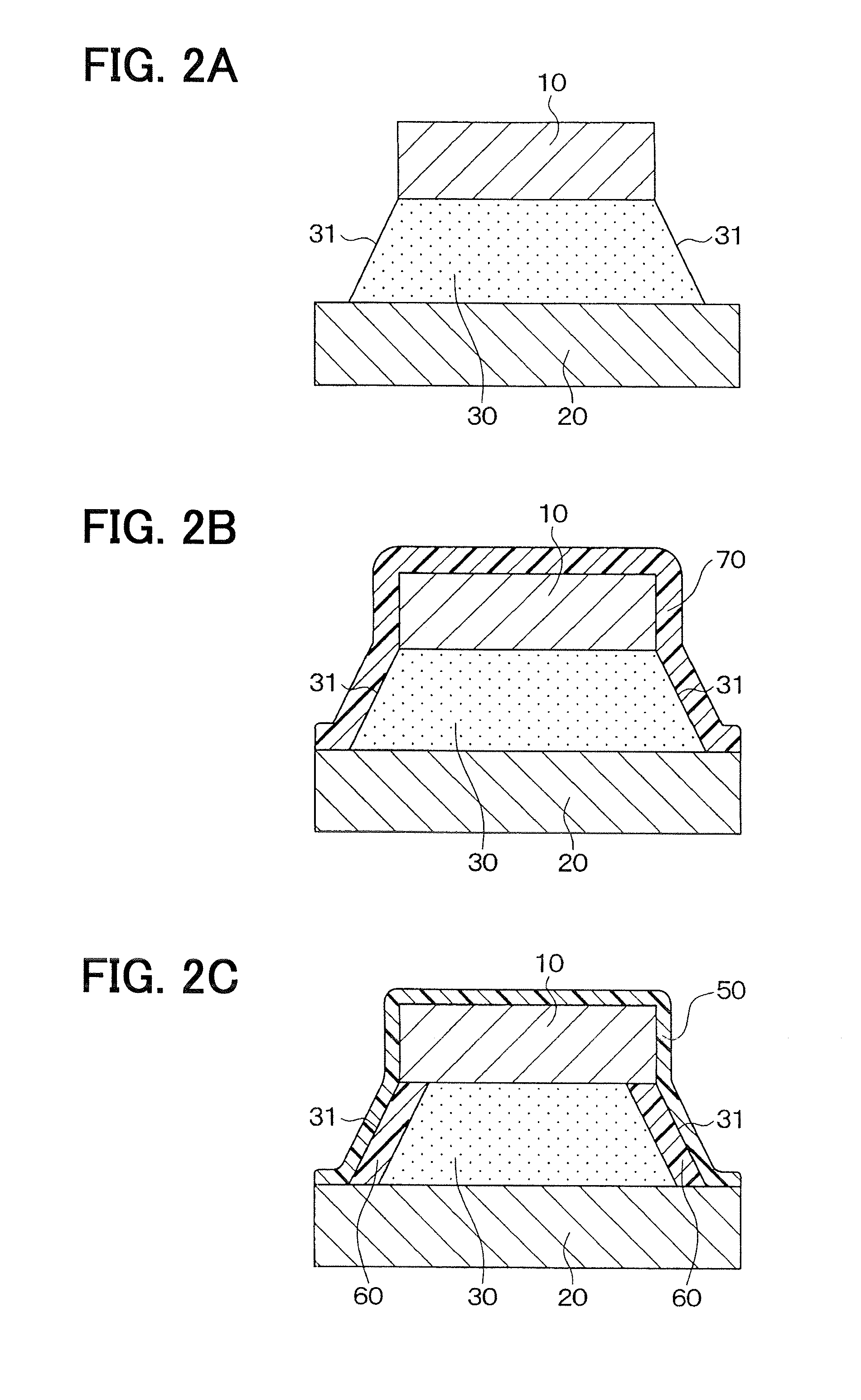
[0082]A second embodiment of the present application will be described with reference to FIG. 1, FIGS. 9A and 9B. FIGS. 9A and 9B are schematic sectional views showing a manufacturing method of an electronic device of the second embodiment. More specifically, FIGS. 9A and 9B show an impregnation process of the reinforcing resin 60, in the manufacturing method of the electronic device. In the second embodiment, different points of the manufacturing method, different from the above-described first embodiment, will be mainly described.

[0083]In the second embodiment, the electronic component 10 and the joining member 20 are mechanically joined via the metal conductor 30, as in the above-described first embodiment. Next, as shown in FIG. 9A, a paste 70, made of polyimide and NMP as a diluent of polyimide, is applied to the electronic component 10, the joining member 20 and the end surface 31 of the metal conductor 30. Here, the polyimide is the material for forming the primer 50 and the ...

third embodiment

[0096]A third embodiment of the present invention will be described with reference to FIGS. 1, 10A and 10B. FIG. 10A is a schematic sectional view showing a manufacturing method of an electronic device of the third embodiment, and FIG. 10B is an enlarged view showing a part of the electronic device around a recess portion 21 of the joining member 20. More specifically, FIG. 10A shows an applying step of the paste 70 for forming the primer 50 and the reinforcing resin 60, in a manufacturing method of the electronic device.

[0097]In the present embodiment, the primer 50 and the reinforcing resin 60 may be made of the same paste 70 (same resin material). In this case, the following method of the present embodiment may be combined with the manufacturing method of the above-described first or second embodiment. In the third embodiment, different points of the manufacturing method, different from the above-described first embodiment, will be mainly described.

[0098]As shown in FIGS. 10A and...


PUM

PropertyMeasurementUnit
impregnation depthaaaaaaaaaa
pore diameteraaaaaaaaaa

Abstract

An electronic device includes an electronic component, a joining member to be mechanically joined with the electronic component, and a metal conductor located between the electronic component and the joining member to mechanically join the electronic component and the joining member. The metal conductor is made of porous noble metal to have pores, and includes an end surface without being covered by the electronic component and the joining member. Furthermore, a reinforcing resin is impregnated from the end surface of the metal conductor to the pores inside of the metal conductor, so as to mechanically reinforce the metal conductor.

Description

CROSS REFERENCE TO RELATED APPLICATION[0001]This application is based on Japanese Patent Application No. 2010-026636 filed on Feb. 9, 2010, the contents of which are incorporated herein by reference in its entirety.FIELD OF THE INVENTION[0002]The present invention relates to an electronic device and a method of manufacturing an electronic device. For example, the electronic device includes an electronic component mechanically joined to a member to be joined via a metal conductor made of a porous noble metal material.BACKGROUND OF THE INVENTION[0003]In an electronic device, an electronic component such as an IC chip or a power element, is mechanically joined to another component such as a wiring board or a lead frame, through a joining material. Furthermore, the mechanically joined components are sealed by using a mold resin[0004]For example, solder such as Pb-free solder which does not contain Pb has been used, in recent years. The electronic component may be used in a high temperat...

Claims


Application Information

Patent Timeline
Patent Type & Authority Applications(United States)
IPC IPC(8): H02G15/02H05K1/09H05K13/00
CPCH01L2224/8384H05K3/284H05K2203/1316Y10T29/49144Y10T29/49117H01L24/32H01L2224/8392H01L2224/83951H05K2203/1322H01L2924/15787H01L23/3135H01L21/56H01L24/83H01L2224/3201H01L2224/32014H01L2224/26175H01L2924/181H01L2924/14H01L2224/83194H01L2924/00H01L2924/00012
Inventor ISHINO, HIROSHIIZUMI, TAKAOTSURUTA, KAZUHIROKATO, NOBUYUKI
Owner DENSO CORP
Why Eureka
Try Eureka