Scanning signal line drive circuit, shift register and display device

a drive circuit and signal line technology, applied in the direction of digital storage, instruments, computing, etc., can solve the problem of not being able to transfer video signals indicating pixels, and achieve the effect of suppressing the degradation of the switching elements provided for discharging the first-node and the output-node, suppressing and effectively preventing the degradation of the switching elements

Inactive Publication Date: 2011-08-11
SHARP KK
View PDF17 Cites 22 Cited by
  • Summary
  • Abstract
  • Description
  • Claims
  • Application Information

AI Technical Summary

Benefits of technology

According to the first aspect of the present invention, in each of the bistable circuits that constitute the shift register within the scanning signal line drive circuit of the display device, regarding the first switching element, the first electrode thereof is connected to the first-node, the second electrode thereof is supplied with the first clock signal, and the third electrode thereof is connected to the output-node. For this reason, when the first clock signal changes from the low level to the high level after a potential of the first-node increases based on the predetermined input signal or the state signal of the previous stage, the potential of the first-node further increases due to a parasitic capacitance between the first electrode and the second electrode of the first switching element, thereby turning the first switching element to the ON state. Therefore, a potential of the output-node increases, and the state signal indicating the first state is outputted from the output-node. The output-node is discharged by the first output-node discharge unit. The potential of the first-node increases based on the first clock signal. Further, each bistable circuit is provided with the first first-node discharge unit and the second first-node discharge unit. Moreover, each bistable circuit is provided with the second-node charge unit for charging the second-node connected to the first electrode of the second switching element included in the second first-node discharge unit, and the first second-node discharge unit for discharging the second-node. As the first first-node discharge unit operates based on the second clock signal or the third clock signal, the first-node is discharged by the first first-node discharge unit during a period in which the second clock signal or the third clock signal is at the high level. During a period in which the first clock signal is at the high level, the first-node should be discharged only during a period other than a period in which the state signal indicating the first state should be outputted from the output-node (selected period). In this regard, during the selected period, the potential of the second-node is decreased by the first second-node discharge unit. As this turns the second switching element to the OFF state, the second first-node discharge unit does not decrease the potential of the first-node during the selected period. In this manner, it is possible to cause the shift register within the scanning signal line drive circuit to perform a desired operation.
Regarding the output-node, it is configured to be connected only to the third electrode of the first switching element included in the output-node charge unit and the first output-node discharge unit. Unlike the conventional example, the first-node and the output-node are not connected by the second electrode and the third electrode of the switching element. For this reason, the change in the potential of the output-node does not affect the first-node. Therefore, even when an off-leak occurs in the first switching element, the potential of the ...

Problems solved by technology

However, it is not possible to transfer video signals indicating pixel values fo...

Method used


Image

  • Scanning signal line drive circuit, shift register and display device
  • Scanning signal line drive circuit, shift register and display device
  • Scanning signal line drive circuit, shift register and display device

Examples


first embodiment

1. First Embodiment

1.1 Overall Configuration and Operation

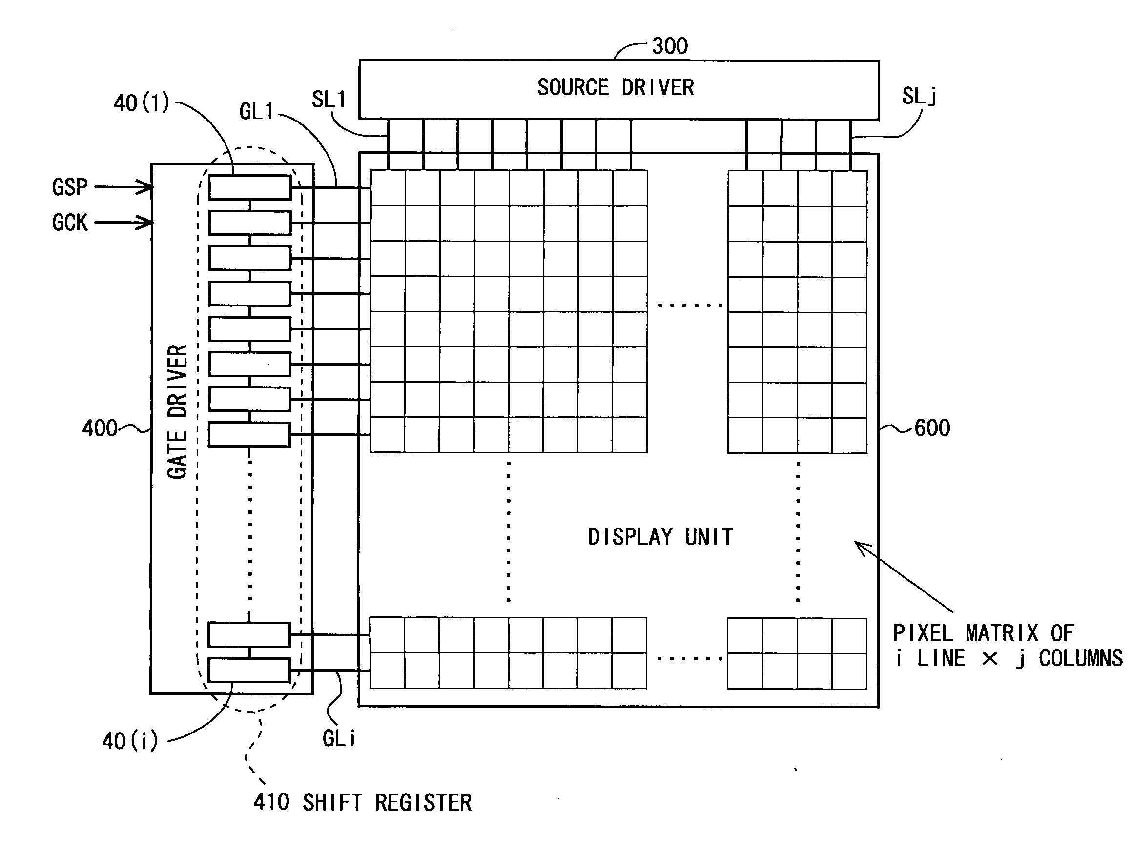
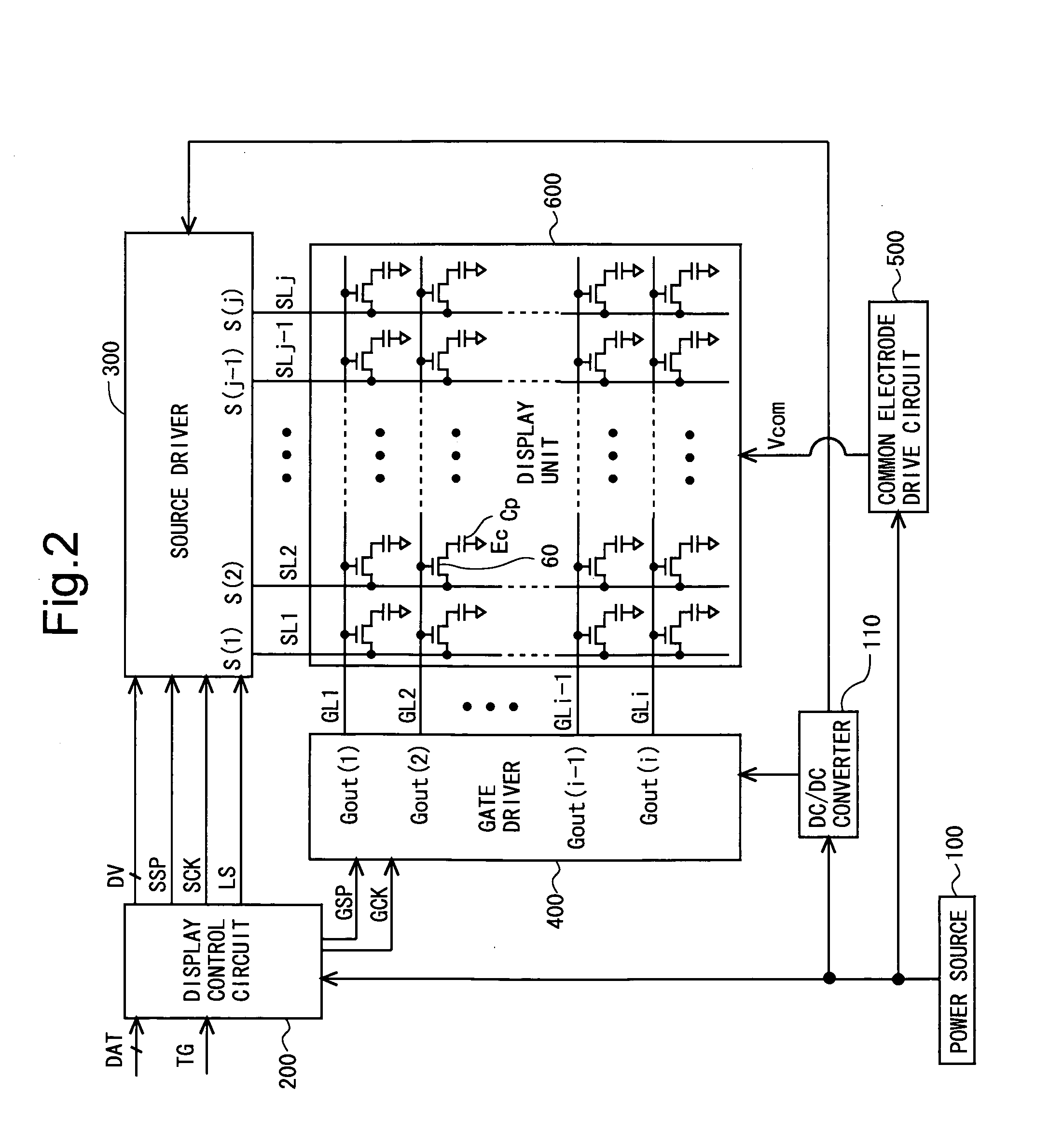
FIG. 2 is a block diagram illustrating an overall configuration of an active matrix-type liquid crystal display device according to a first embodiment of the present invention. As shown in FIG. 2, the liquid crystal display device is provided with a power source 100, a DC / DC converter 110, a display control circuit 200, a source driver (video signal line drive circuit) 300, a gate driver (scanning signal line drive circuit) 400, a common electrode drive circuit 500, and a display unit 600. Typically, the display unit 600 and the gate driver 400 as a drive circuit are formed on the same substrate, i.e., monolithically.

The display unit 600 includes a plurality of (j) source bus lines (video signal lines) SL1 to SLj, a plurality of (i) gate bus lines (scanning signal line) GL1 to GLi, and a plurality of (i×j) pixel formation portions respectively provided at intersections of the source bus lines SL1 to SLj and the gate bus lin...

second embodiment

2. Second Embodiment

2.1 Overall Configuration and the Like

An overall configuration, a configuration in outline of a gate driver, and a configuration of a shift register according to this embodiment are the same as those described in the first embodiment with reference to FIG. 2 to FIG. 4, and therefore explanations thereof are omitted. Further, waveforms of first to third gate clock signals as well as of scanning signals are the same as those described in the first embodiment with reference to FIG. 5 and FIG. 6, and therefore explanations thereof are omitted.

2.2 Configuration and Operation of Bistable Circuit

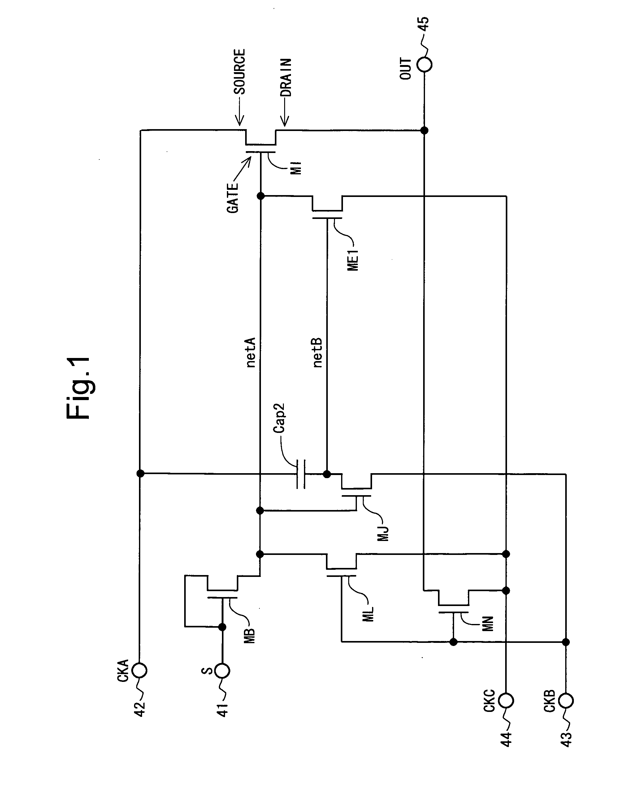
FIG. 12 is a circuit diagram illustrating a configuration of a bistable circuit according to this embodiment. In this embodiment, a thin film transistor MK1 (ninth switching element) and a capacitor Cap1 are provided, in addition to the components described in the first embodiment with reference to FIG. 1. Regarding the thin film transistor MK1, a gate terminal thereof is connec...

third embodiment

3. Third Embodiment

3.1 Overall Configuration and the Like

An overall configuration and a configuration in outline of a gate driver according to this embodiment are the same as those described in the first embodiment with reference to FIG. 2 and FIG. 3, and therefore explanations thereof are omitted. Further, waveforms of first to third gate clock signals as well as of scanning signals are the same as those described in the first embodiment with reference to FIG. 5 and FIG. 6, and therefore explanations thereof are omitted.

FIG. 14 is a block diagram illustrating a configuration of the shift register 410 within the gate driver 400 according to this embodiment. In this embodiment, each bistable circuit is provided with an input terminal for receiving a reset signal R, in addition to the input terminals and the output terminal described in the first embodiment. In addition, the input terminal for receiving the reset signal R is configured to be supplied with the state signal OUT that is ...


PUM


Abstract

There is provided a display device capable of preventing a malfunction and a display defect due to an off-leak from occurring even when a circuit in a shift register is configured utilizing thin film transistors of relatively large off-leaks. In at least one embodiment, each of bistable circuits that constitute the shift register includes: a thin film transistor for increasing a potential of an output terminal based on a first clock; a thin film transistor for decreasing the potential of the output terminal; a thin film transistor for increasing a potential of a range netA connected to a gate terminal of the thin film transistor based on a start signal; thin film transistors for decreasing the potential of the range netA; a capacitor for increasing the potential of a range netB connected to a gate terminal of the thin film transistor; and a thin film transistor for decreasing the potential of the range netB.

Description

TECHNICAL FIELDThe present invention relates to a display device and a drive circuit thereof, and, in particular, to a shift register within a scanning signal line drive circuit that drives scanning signal lines provided within a display unit of the display device.BACKGROUND ARTLiquid crystal display devices utilizing amorphous silicon thin film transistors (hereinafter referred to as “a-Si TFTs”) as driver elements have conventionally been known. In recent years, development of liquid crystal display devices utilizing microcrystalline silicon thin film transistors (hereinafter referred to as “μc-Si TFTs”) as driver elements is moving forward. Mobility of microcrystalline silicon is greater than that of amorphous silicon, and the μc-Si TFTs can be formed by a process similar to that of the a-Si TFTs. For this reason, employment of the μc-Si TFTs as the driver elements is expected to realize such as a cost reduction by decreasing a frame area, a cost reduction by decreasing a number ...

Claims


Application Information

Patent Timeline
IPC IPC(8): G09G5/00G11C19/00
CPCG09G3/3677G11C19/28G11C19/184G09G2310/0286
Inventor SAKAMOTO, MAYUKOIWASE, YASUAKINAKATANI, YOSHIKITAKAHASHI, YOSHIHISA
Owner SHARP KK
Why Eureka
Try Eureka