Semiconductor device and driving method thereof

a technology of electromagnetic field and driving method, which is applied in the direction of radio frequency controlled devices, instruments, television systems, etc., can solve the problems of deterioration of sensitivity, small area occupied by display elements, and noise at image pick-up time, so as to achieve low noise and high resolution

Inactive Publication Date: 2011-08-18
SEMICON ENERGY LAB CO LTD
View PDF11 Cites 54 Cited by
  • Summary
  • Abstract
  • Description
  • Claims
  • Application Information

AI Technical Summary

Benefits of technology

[0022]According to one embodiment of the present invention, a semiconductor device equipped with a high-quality image pick-up function and / or a high-quality display function with high resolution and with less noise can be provided.

Problems solved by technology

Contraction of design rules causes deterioration of sensitivity of receiving light due to area reduction of a light-receiving portion of a light-receiving element (photodiode), leading to noise at the time of image pick-up.
In addition, the semiconductor device having a photosensor in a display region has had a problem in that an area occupied by a display element is small and the display quality is insufficient because a display element portion for displaying an image and a photosensor portion for detecting an object are both provided in a pixel.

Method used


Image

  • Semiconductor device and driving method thereof
  • Semiconductor device and driving method thereof
  • Semiconductor device and driving method thereof

Examples


embodiment 1

[0041]In Embodiment 1, one example of a semiconductor device according to one embodiment of the present invention will be described using drawings.

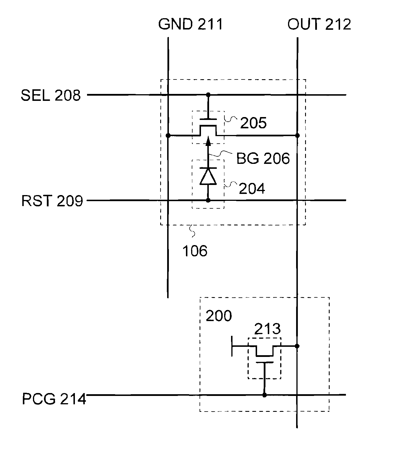
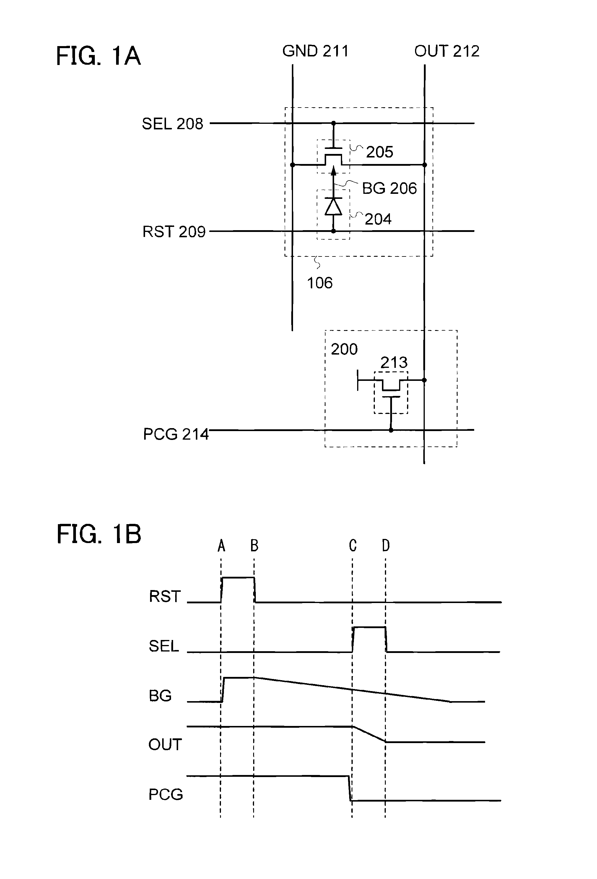
[0042]FIG. 1A illustrates a configuration for one pixel, of photosensors arranged in pixel matrix of a semiconductor device equipped with an image pick-up function, which includes a photodiode 204 and a transistor 205.

[0043]An anode of the photodiode 204 is electrically connected to a photodiode reset signal line (hereinafter referred to as a reset signal line) 209, and a cathode thereof is electrically connected to a back-gate signal line 206. One of a source and a drain of the transistor 205, the other of the source and the drain thereof, a gate thereof, and a back gate thereof are electrically connected to a photosensor reference signal line (hereinafter referred to as a reference signal line) 211, a photosensor output signal line (hereinafter referred to as an output signal line) 212, a gate signal line (hereinafter referred to as a s...

embodiment 2

[0084]In Embodiment 2, a photosensor having a configuration different from Embodiment 1 will be described.

[0085]The photosensor in this embodiment further includes one transistor in the photosensor described in Embodiment 1. Therefore, Embodiment 1 can be referred to for the portion common to the photosensor described in Embodiment 1.

[0086]FIG. 15 illustrates a configuration for one pixel, of photosensors arranged in pixel matrix of a semiconductor device equipped with an image pick-up function, which includes a photodiode 404, a first transistor 405, and a second transistor 406.

[0087]An anode of the photodiode 404 is electrically connected to a photodiode reset signal line (hereinafter referred to as a reset signal line) 409, and a cathode thereof is electrically connected to a wiring 407. A gate of the first transistor 405, one of a source and a drain thereof, and the other of the source and the drain thereof are electrically connected to a gate signal line (hereinafter referred t...

embodiment 3

[0122]In Embodiment 3, an example of a transistor which can be applied to a semiconductor device disclosed in this specification will be described.

[0123]There is no particular limitation on a structure of a transistor which can be applied to the semiconductor device disclosed in this specification: for example, a top-gate structure or a bottom-gate structure such as a staggered type and a planar type can be used. Further, the transistor may have a single gate structure including one channel formation region, a double gate structure including two channel formation regions, or a triple gate structure including three channel formation regions.

[0124]Examples of a cross-sectional structure of the transistor shown in FIGS. 5A to 5D are described below. One embodiment of the present invention features in that as a back-gate electrode a conductive layer which is formed so as to face a gate electrode of the transistor with a gate insulating film, a semiconductor layer serving as a channel fo...


PUM


Abstract

A transistor a gate of which, one of a source and a drain of which, and the other are electrically connected to a selection signal line, an output signal line, and a reference signal line, respectively and a photodiode one of an anode and a cathode of which and the other are electrically connected to a reset signal line and a back gate of the transistor, respectively are included. The photodiode is forward biased to initialize the back-gate potential of the transistor, the back-gate potential is changed by current of the inversely-biased photodiode flowing in an inverse direction in accordance with the light intensity, and the transistor is turned on to change the potential of the output signal line, so that a signal in accordance with the intensity is obtained.

Description

TECHNICAL FIELD[0001]Embodiments of the present invention relate to a semiconductor device in which pixels having a photosensor are arranged in matrix and to a driving method thereof. Further, an embodiment of the present invention relates to an electronic appliance having the semiconductor device.BACKGROUND ART[0002]A semiconductor device in this specification refers to any device that can function by utilizing semiconductor characteristics; electro-optic devices, semiconductor circuits, and electronic appliances are all semiconductor devices.[0003]In recent years, a semiconductor device having a sensing element for detecting light (also called a “photosensor”) has drawn attention. As examples of the semiconductor device having a photosensor, a CCD image sensor, a CMOS image sensor, and the like can be given. They are used in electronic appliances equipped with an image pick-up function such as a digital still camera and a mobile phone.[0004]A semiconductor device having a photosen...

Claims


Application Information

Patent Timeline
Patent Type & Authority Applications(United States)
IPC IPC(8): H01L31/032G01J1/44
CPCG02F1/13318H01L27/146G06F3/0412H01L27/14632H01L27/14643H01L27/14678H04N5/3745A61B5/1172G02F1/133512G02F1/133615G02F1/136209G02F2001/13356G02F2001/133622G02F2001/13685H04N1/195H01L29/7869G06K9/0002H01L27/1225G09G3/3648G09G2320/0666G09G2360/145G02F1/13338G06F3/042G02F1/13356G02F1/133622G02F1/13685G06V40/1306H04N25/77G06F3/04164
Inventor KUROKAWA, YOSHIYUKI
Owner SEMICON ENERGY LAB CO LTD
Why Eureka
Try Eureka