
Charge transport layers and organic electron devices comprising same

a charge transport layer and electron transport technology, applied in the direction of non-metal conductors, conductors, nanoinformatics, etc., can solve the problems of difficult multilayer deposition by solution processing, limited charge injection and transport properties of these materials, and relatively low conductivity of most hole transport or electron transport materials

Inactive Publication Date: 2011-08-18
EI DU PONT DE NEMOURS & CO
View PDF39 Cites 10 Cited by
  • Summary
  • Abstract
  • Description
  • Claims
  • Application Information

AI Technical Summary

Benefits of technology

The use of doped layers leads to enhanced charge injection and transport efficiency, enabling the creation of high-performance organic electronic devices with improved conductivity and stability, particularly in multilayer deposition processes.

Problems solved by technology

Most of the hole transport or electron transport materials, however, have relatively low conductivity due to the intrinsic properties of these charge transport materials.
Thus, the performance of the charge injection and transport properties of these materials are limited in achieving high efficiency organic electronic devices.
It is also known in the art that the hole transporting and electron transporting materials are generally soluble in common organic solvents, which can make it difficult to use them for multilayer deposition by solution processing.

Method used

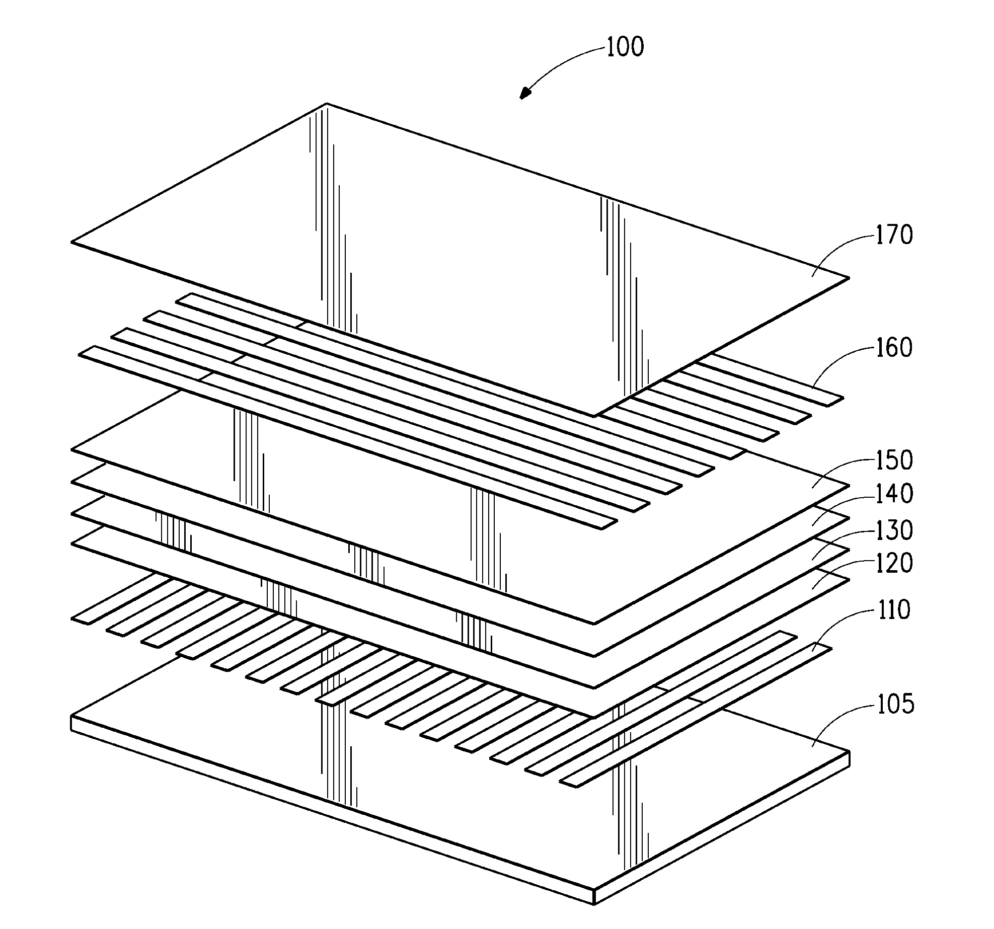
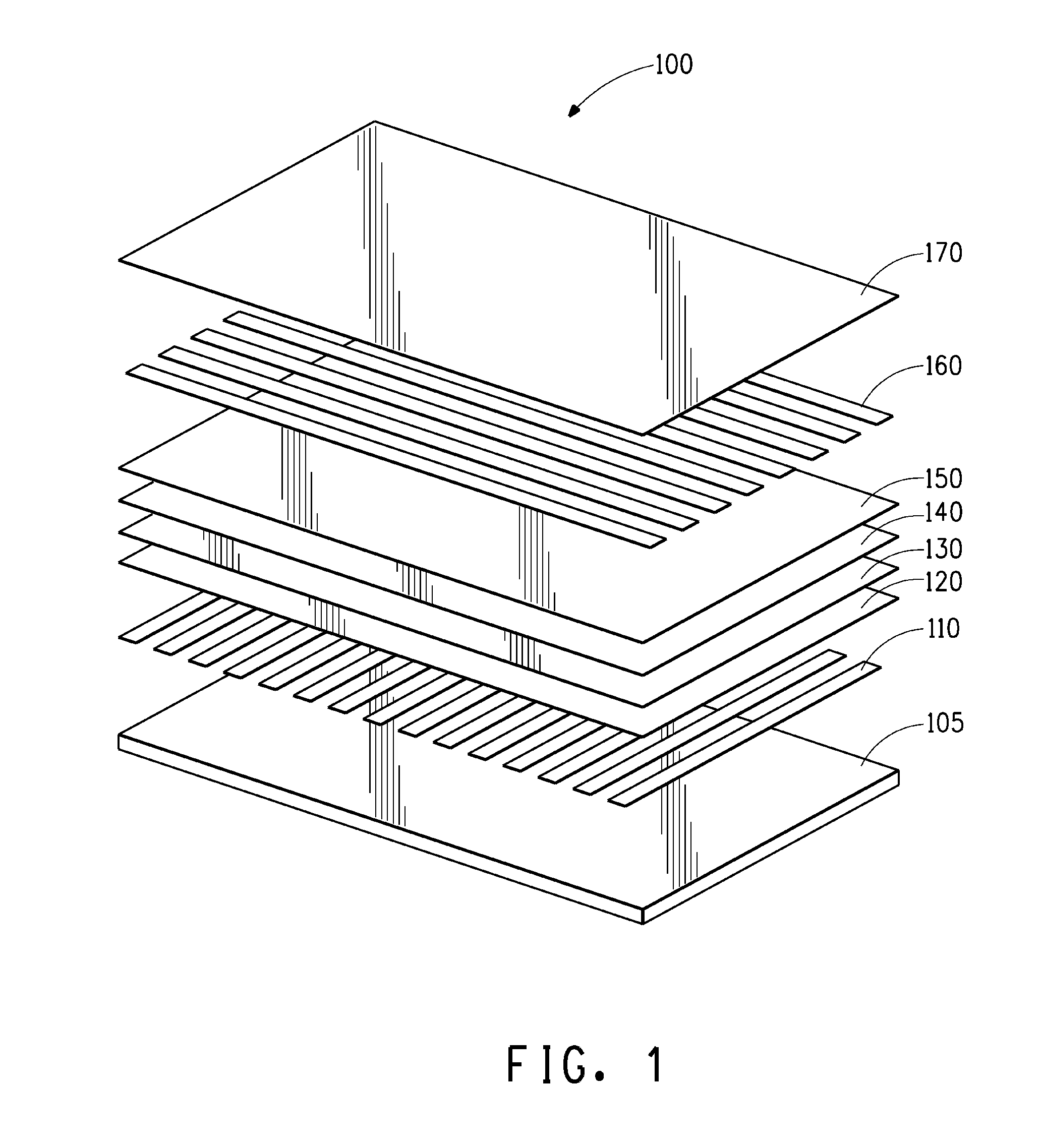

Image

  • Charge transport layers and organic electron devices comprising same
  • Charge transport layers and organic electron devices comprising same
  • Charge transport layers and organic electron devices comprising same

Examples


example 1

[0113]This example illustrates a p-doped hole injection material (or complex):

[0114]In the above case hole transport material m-OMTDATA is doped with electron deficient F4-TCNQ in a ratio of 2˜200:1 to form a p-doped hole injection material. The complex in various ratio will be tested for solubility in various solvents other than the common organic solvents for photoactive materials.

example 2

[0115]This example illustrates a n-doped electron injection material:

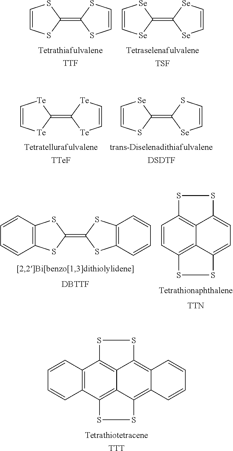
[0116]In the above case electron transport material FQP is doped with electron rich TTT in a ratio of 2-200:1 to form a n-doped electron injection material. The complex in various ratio will be tested for solubility in various solvents other than the common organic solvents for photoactive materials.

example 3

[0117]This example illustrates a p-doped hole injection material. The hole injection material is a crosslinked polymer, P5 doped with C60.

(a) Synthesis of P5

[0118]This example demonstrates the preparation of hole transport material P5.

Synthesis of Compound 2

[0119]Under an atmosphere of nitrogen, a 250 mL round bottom was charged with 9,9-dioctyl-2,7-dibromofluorene (25.0 g, 45.58 mmol), phenylboronic acid (12.23 g, 100.28 mmol), Pd2(dba)3 (0.42 g, 0.46 mmol), PtBu3 (0.22 g, 1.09 mmol) and 100 mL toluene. The reaction mixture stirred for five minutes after which KF (8.74 g, 150.43 mmol) was added in two portions and the resulting solution was stirred at room temperature overnight. The mixture was diluted with 500 mL THF and filtered through a plug of silica and celite and the volatiles were removed from the filtrate under reduced pressure. The yellow oil was purified by flash column chromatography on silica gel using hexanes as eluent. The product was obtained as a white solid in 80....


PUM

PropertyMeasurementUnit
temperatureaaaaaaaaaa
electrical energyaaaaaaaaaa
conductivityaaaaaaaaaa

Abstract

Provided are organic n-doped electron transport layers comprising at least one electron transport material and at least one electron rich dopant material and organic p-doped hole transport layers comprising at least one hole transport material and at least one electron deficient dopant material.

Description

CROSS-REFERENCE TO RELATED APPLICATIONS[0001]The present application is a Continuation-in-Part of U.S. application Ser. No. 11 / 319,940, filed Dec. 28, 2005, which claims priority to U.S. Provisional Application Ser. Nos. 60 / 640,540, filed Dec. 30, 2004 and 60 / 694,939, filed Jun. 28, 2005.FIELD OF THE DISCLOSURE[0002]This disclosure relates generally to electronic devices comprising charge transport layers.BACKGROUND INFORMATION[0003]Organic electronic devices convert electrical energy into radiation, detect signals through electronic processes, or convert radiation into electrical energy. Organic Light Emitting Diodes (OLEDs) are one class of organic electronic devices. Some simple OLEDs have the following structure, in order, anode, hole transporting layer, light emitting material layer, electron transporting layer and cathode. Most of the hole transport or electron transport materials, however, have relatively low conductivity due to the intrinsic properties of these charge transp...

Claims


Application Information

Patent Timeline
Patent Type & Authority Applications(United States)
IPC IPC(8): H01L33/26H01L29/02H01B1/12B05D5/12B05D3/00
CPCB82Y10/00H01L51/002H01L51/0039H01L51/0046H01L51/5052H01L51/0054H01L51/0059H01L51/0071H01L51/0072H01L51/0051H10K71/30H10K85/115H10K85/211H10K85/611H10K85/622H10K85/631H10K85/657H10K85/6572H10K50/155H10K50/165
Inventor PRAKASH, SHIVAHSU, CHE-HSIUNG
Owner EI DU PONT DE NEMOURS & CO
Learn More