Manufacturing method of semiconductor device

a manufacturing method and semiconductor technology, applied in semiconductor devices, semiconductor/solid-state device details, electrical devices, etc., can solve the problems of reducing the productivity of semiconductor devices, deteriorating quality or productivity, and lowering the adhesion properties of semiconductor devices, so as to improve the reliability of semiconductor devices

Inactive Publication Date: 2011-08-18
RENESAS ELECTRONICS CORP
View PDF1 Cites 21 Cited by
  • Summary
  • Abstract
  • Description
  • Claims
  • Application Information

AI Technical Summary

Benefits of technology

[0012]The following explains briefly the effect acquired by one embodiment of the typical invention among the inventions disclosed in the present application.
[0013]The dete

Problems solved by technology

In BGA (Ball Grid Array) or LGA (Land Grid Array), there occurs such a problem as quality deterioration or productivity lowering caused by gasification of a part of components of materials constituting the wiring substrate in the manufacturing process.
(3) The contamination of the surface of the semiconductor chip by

Method used


Image

  • Manufacturing method of semiconductor device
  • Manufacturing method of semiconductor device
  • Manufacturing method of semiconductor device

Examples


Embodiment Construction

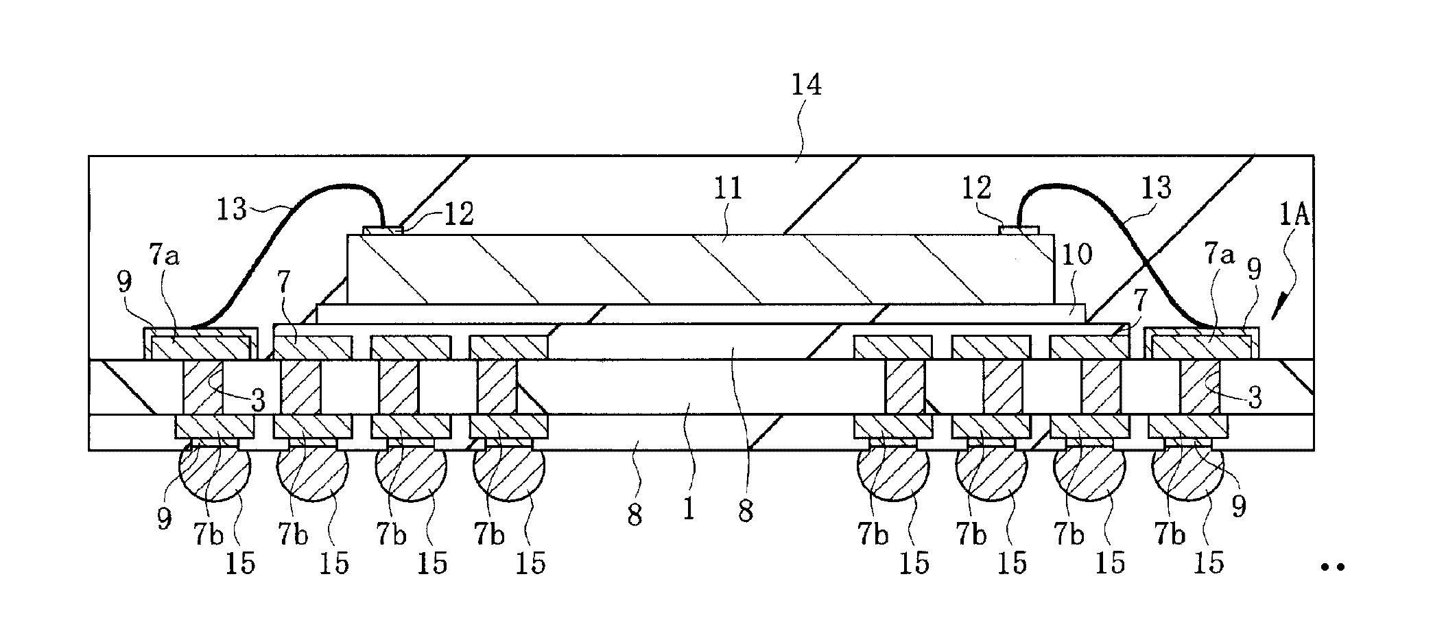
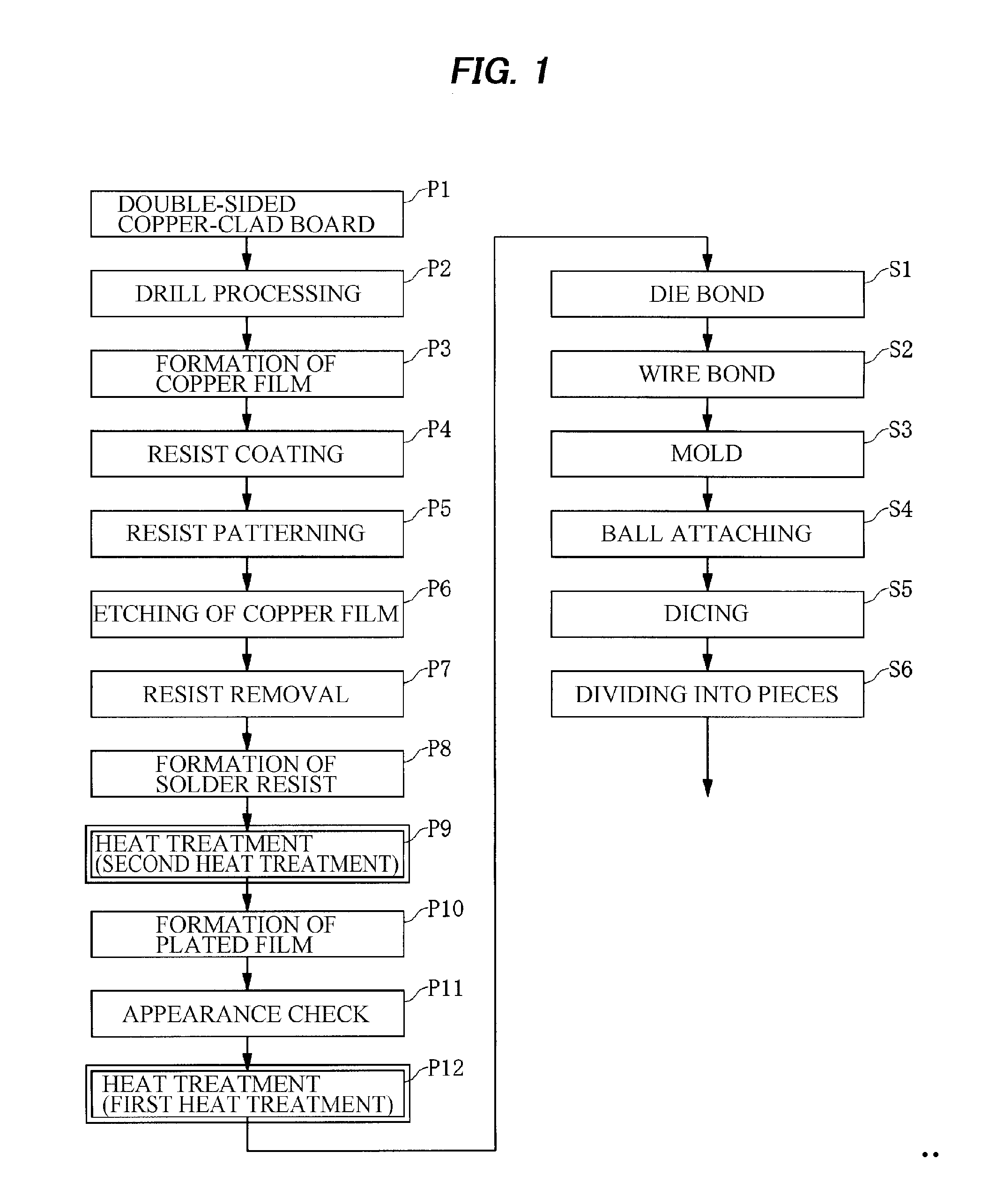
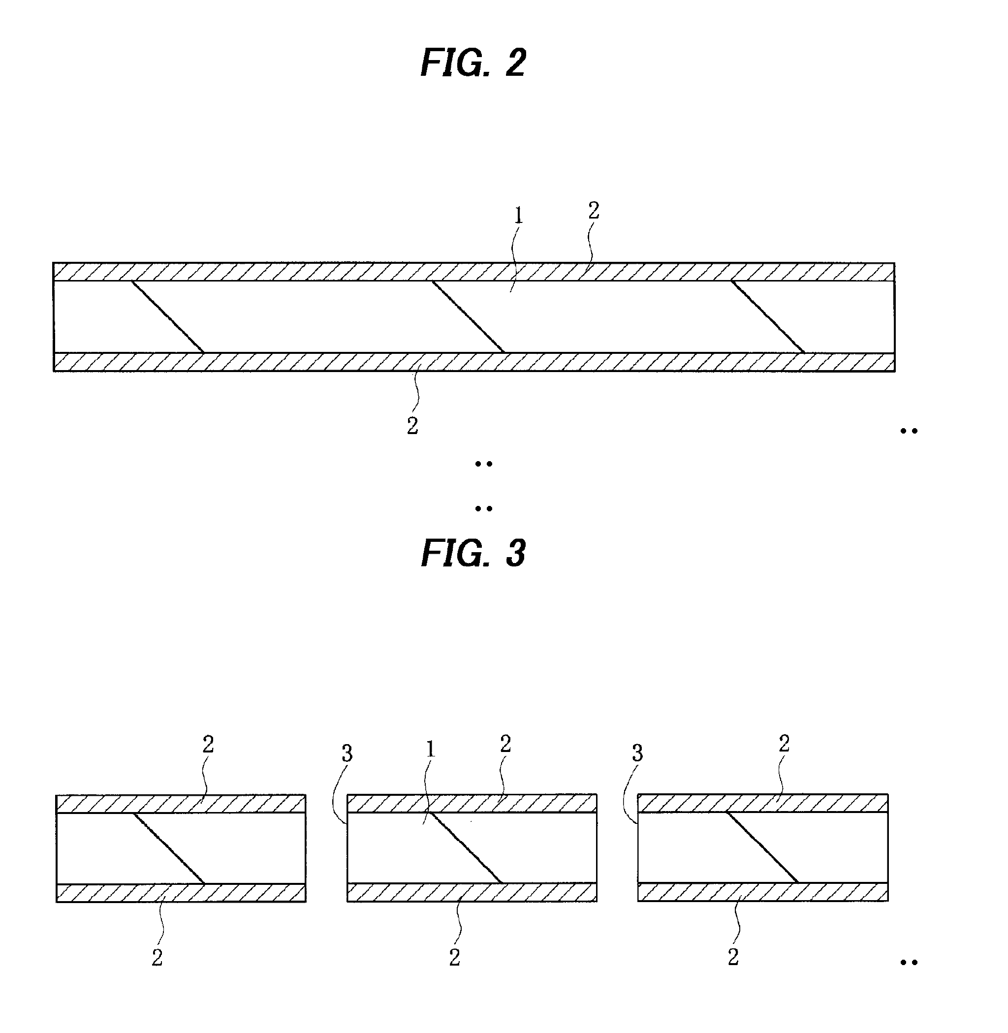
[0033]The following embodiments will be explained, divided into plural sections or embodiments, if necessary for convenience. Except for the case where it shows clearly in particular, they are not mutually unrelated and one has relationships such as a modification, details, and supplementary explanation of some or entire of another.

[0034]In the following embodiments, when referring to the number of elements, etc. (including the number, a numeric value, an amount, a range, etc.), they may be not restricted to the specific number but may be greater or smaller than the specific number, except for the case where they are clearly specified in particular and where they are clearly restricted to a specific number theoretically. Furthermore, in the following embodiments, it is needless to say that an element (including an element step etc.) is not necessarily indispensable, except for the case where it is clearly specified in particular and where it is considered to be clearly indispensable...


PUM

PropertyMeasurementUnit
Temperatureaaaaaaaaaa

Abstract

To provide a technology capable of preventing the deterioration of the reliability of semiconductor devices caused by the gasification of a part of components of the material constituting a wiring substrate.
A wiring layer constituting a circuit pattern is formed over each of the front and rear surfaces of a glass epoxy substrate, and after the formation of a solder resist covering the wiring layer while exposing a part of the wiring layer and prior to a heat treatment (first heat treatment) at 100° C. to 150° C. for dehumidification, a heat treatment (second heat treatment) at 160° C. to 230° C. for gasifying and discharging an organic solvent contained in the material constituting a wiring substrate is performed for the wiring substrate.

Description

CROSS-REFERENCE TO RELATED APPLICATION[0001]The disclosure of Japanese Patent Application No. 2010-30336 filed on Feb. 15, 2010 including the specification, drawings and abstract is incorporated herein by reference in its entirety.BACKGROUND OF THE INVENTION[0002]The present invention relates to a manufacturing technology of a semiconductor device, in particular, to a technology useful when applied to a manufacturing method of a semiconductor device having a process of mounting a semiconductor chip over the surface of a wiring substrate.[0003]For example, Japanese Patent Laid-Open No. 1998-41337 (Patent Document 1) discloses a manufacturing method of a mounting substrate, in which a glass epoxy substrate is previously subjected to burn-in in a high-temperature dry atmosphere, coated with a moisture-resistant resin material, and, after that, the moisture-resistant resin material is also coated over the cut surface and hole wall of the glass epoxy resin. In the burn-in, for example, t...

Claims


Application Information

Patent Timeline
IPC IPC(8): H01L21/786H01L21/60H01L21/56H01L21/58H01L21/00
CPCH01L2924/01005H01L23/544H01L2924/0133H01L2224/85444H01L2224/45144H01L2924/01014H01L2924/01013H01L2924/01074H01L2224/73265H01L2224/48091H01L2924/0665H01L2224/83101H01L24/45H01L2223/54406H01L23/296Y10T29/41H01L2924/01079H01L2924/01004H01L2224/48465H01L2924/01047H01L2924/01082H01L2924/01078H01L2924/15311H01L2224/85205H01L23/295H01L24/97H01L2924/01033H01L2924/014H01L2224/85203H01L2924/12044H01L2224/2919H01L2223/54486H01L2924/01006H01L2224/83192H01L2224/32225H01L2924/00014H01L2224/838H01L2924/1579H01L24/85H01L21/4853H01L2924/01029H01L2224/29111H01L24/48H01L23/3128H01L2224/48227H01L24/83H01L2224/48599H01L2224/92247H01L23/49827H01L2924/01028H01L2924/0105H01L23/49816H01L2224/92H01L2224/97H01L2224/83H01L2224/85H01L2924/00H01L2224/78H01L2924/00012H01L2224/32013H01L2224/48644H01L2924/181H01L2924/12042H01L24/73
Inventor KURODA, SOSHIYASUNAGA, MASATOSHIMATSUSHIMA, HIRONORIHIRONAGA, KENYA
Owner RENESAS ELECTRONICS CORP
Why Eureka
Try Eureka