Integrated doherty amplifier

Active Publication Date: 2011-08-25
AMPLEON NETHERLANDS
View PDF7 Cites 29 Cited by
  • Summary
  • Abstract
  • Description
  • Claims
  • Application Information

AI Technical Summary

Benefits of technology

[0013]The so-called “electrical memory effect” reveals itself as additional inter-modulation distortions of the amplified signal. The effect stems from the non-constant voltage of the power supply at the drain of the power device, which happens at peak power levels. The reason for that is a large value of “choke” inductance, or quarter wavelength transmission line, which is traditionally used for connecting the device's drain to the closest capacitor of the DC power supply. This inductance or transmission line isolates the RF signal path from the DC supply path, and in fact operates as a low-pass filter. If an RF signal is not modulated and has constant or non-variable amplitude (or a constant RF envelope), then the requirements imposed on the choke inductance are somewhat relaxed. The choke inductance can be large, providing a very high impedance looking into the DC power supply path and, as a result, low losses of the RF signal. But if the modulated signal is amplified, then the value of the choke inductance is limited by two contradictory requirements. On the one hand, the inductance must be large enough to provide a high impedance to the amplified RF signal. Typically, the impedance should be larger by two orders of magnitude than required for the RF signal path to allow less than 1% of efficiency loss. On the other hand, this inductance must be small enough to provide minimal impedance for the highest frequency of the spectrum of the modulation signal, typically smaller than 0.3 Ohm at 100 MHz modulation frequency for a 100 W device, to avoid the variations of the power supply voltage at the device's drain. With the traditional way of connecting the device to the DC power supply through an inductance or by a quarter-wave length transmission line, this requirement can be met only at 20-40 MHz at the highest, and this is well below the requirements for a WiMAX communication system. The reason for that is that the choke inductance is too large (at least several nano-Henry). The situation can be resolved if an INSHIN-inductance is used as choke, as a result of which the DC power supply can be connected to a capacitor used in the INSHIN device as a grounding. The INSHIN-, or compensation-, inductance is typically about 0.25 nH for a 100 W device, and is in general several times smaller than the minimal possible traditional choke inductance of 3-4 nH. This allows to minimize the electrical memory effects even at 100 MHz of the modulation signal.
[0014]An embodiment of the circuit of the invention is specified in claim 2. The components are distributed over multiple substrates. One o

Problems solved by technology

A first consideration relates to the fact that the highly-doped silicon substrate used in LDMOS does not allow creating integrated high-quality inductances.
Such inductances introduce losses that directly affect the gain of an integrated Doherty amplifier.
A second consideration relates to the fact that bond pads, arranged on highly doped substrate, introduce parasitic capacitances and also signal losses.
So, if an inductance is needed where more than one bond wire is required with intermediate bond pads, then a non-desired impedance transformation or a phase-shift will occur, and also additional signal losses will be introduced in such an inductance.
As a result, the CLC transmission line and

Method used


Image

  • Integrated doherty amplifier
  • Integrated doherty amplifier
  • Integrated doherty amplifier

Examples


Example

[0026]Throughout the Figures, similar or corresponding features are indicated by same reference numerals.

DETAILED EMBODIMENTS

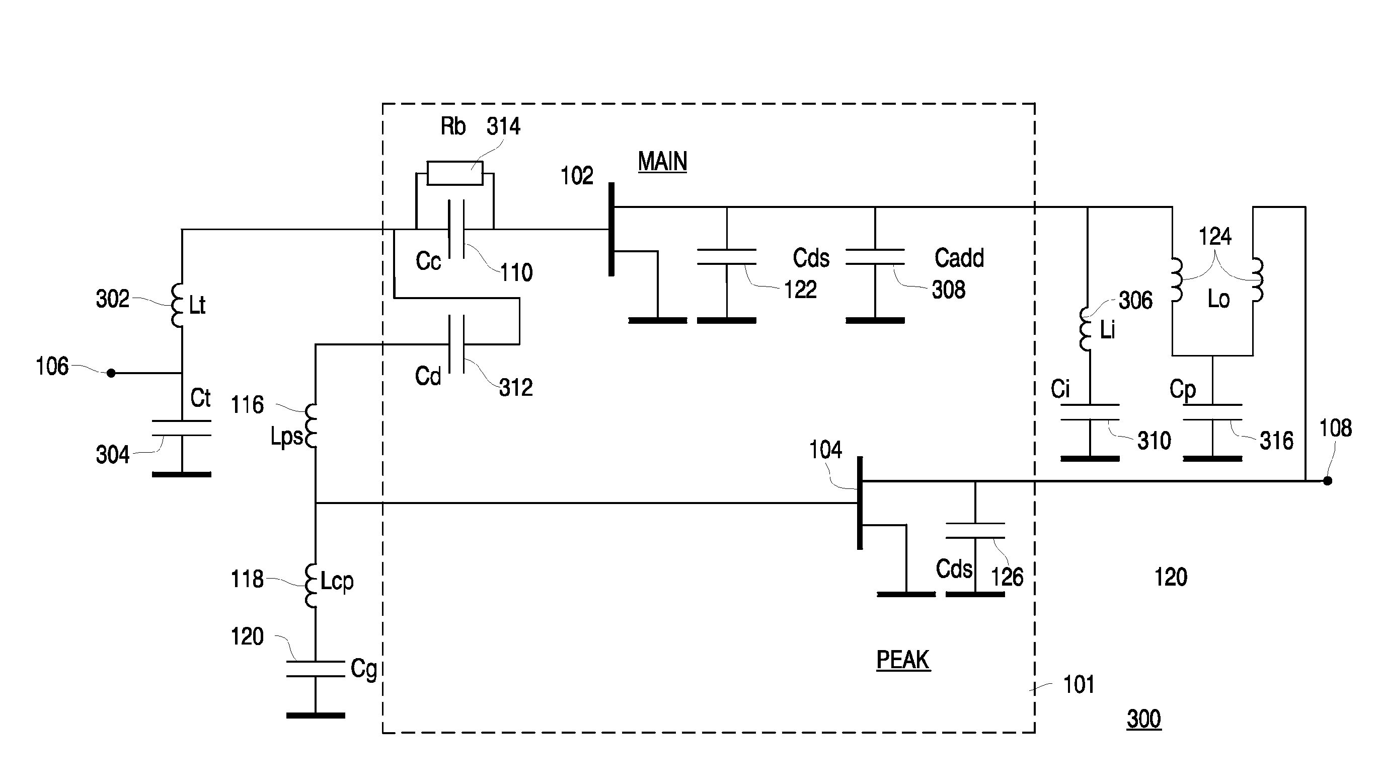
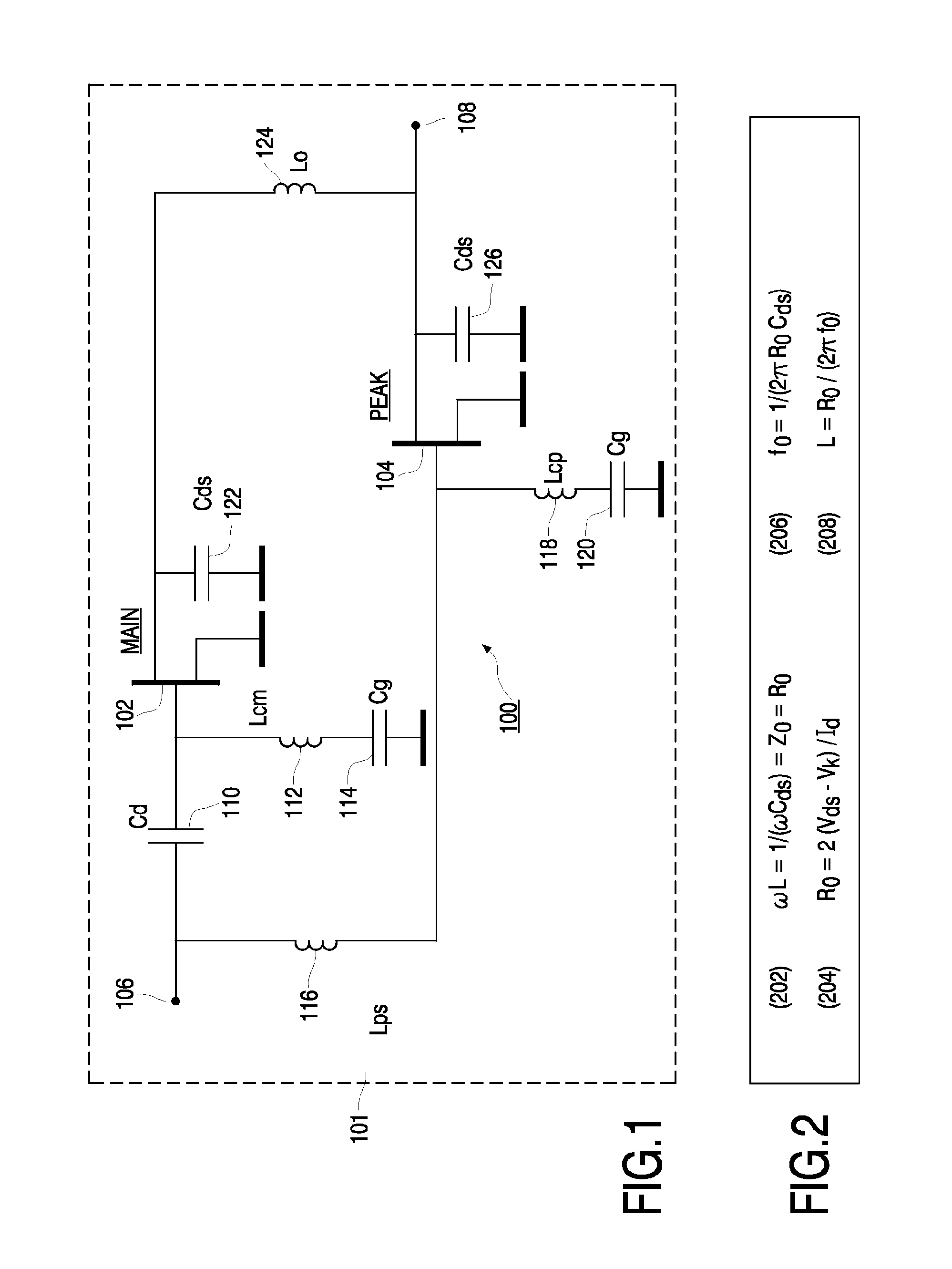
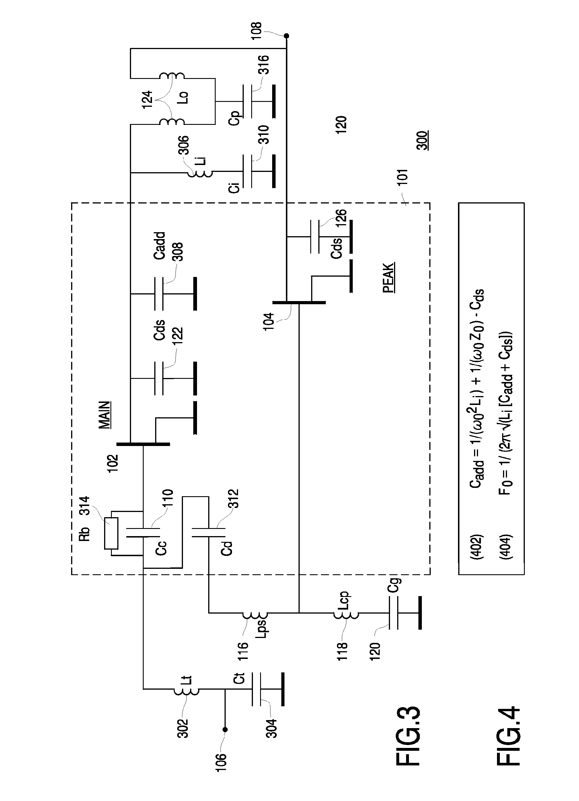
[0027]When modifying the design of cell 100 for operation in these other frequency ranges, the following should be taken into consideration. A first consideration relates to the fact that the highly-doped silicon substrate used in LDMOS does not allow creating integrated high-quality inductances. Typically, the best quality factor (Q-factor) of around 6 is attainable at a frequency of 2 GHz. At all other frequencies, above or below, the quality factor is lower. Such inductances in the input network introduce direct losses that directly affect the gain of an integrated Doherty amplifier. In the output network, such integrated inductances will also affect the gain, as well as power capability and efficiency.

[0028]A second consideration relates to the belief that an integrated Doherty amplifier device is going to be commercially successful only if the device outl...


PUM


Abstract

The invention relates to an integrated Doherty amplifier with an input network connecting the input to the main stage and to the peak stage, and with an output network connecting the main stage and the peak stage to the output. The output network has a shunt capacitor to signal-ground in parallel to a parasitic capacitance of the main stage, and has a shunt inductor between the main stage and signal ground. The shunt configuration enables to use the MMIC Doherty amplifier in a wide frequency range. At least some of the inductors of the input network and/or output network are implemented using bond wires. Their orientations and locations provide minimal mutual electromagnetic coupling between the wires and the return RF current paths.

Description

FIELD OF THE INVENTION[0001]The invention relates to an electronic circuit with a Doherty amplifier.BACKGROUND ART[0002]As known, a classical Doherty amplifier has two amplifying devices arranged in parallel and of the same power capability. The first one of the devices (main stage) operates in a class-AB amplifier mode and the second one (peak stage) operates in a class-C amplifier mode. These devices are separated at their inputs and at their outputs by 90° phase-shifting networks. The output phase-shifting network has a specific characteristic impedance Z0 which must be equal to the optimal load impedance RLm of the main stage. The input signal is split so as to drive the two amplifiers, and a summing network, known as an “impedance inverter” or a “Doherty combiner”, is operative to: a) combine the two output signals, b) to correct for phase differences between the two output signals, and c) to provide an inverted impedance at the output of the Doherty amplifier with respect to t...

Claims


Application Information

Patent Timeline
IPC IPC(8): H03F3/68
CPCH03F3/195H03F1/0288H01L2224/48137
Inventor BLEDNOV, IGOR
Owner AMPLEON NETHERLANDS
Why Eureka
Try Eureka