Semiconductor light emitting device having multi-cell array and method for manufacturing the same

a light-emitting device and semiconductor technology, applied in the direction of discharge tube luminescnet screen, lighting and heating apparatus, light-emitting support devices, etc., can solve the problems of high-power leds using high rated currents that may have low light efficiency, accelerate light efficiency degradation, and reduce power consumption. , the effect of increasing the current density

Inactive Publication Date: 2011-09-01
SAMSUNG ELECTRONICS CO LTD
View PDF8 Cites 36 Cited by
  • Summary
  • Abstract
  • Description
  • Claims
  • Application Information

AI Technical Summary

Benefits of technology

[0008]An aspect of the present invention provides a semiconductor light emitting device which can improve light efficiency by increasing current density per unit area, and can emit white light having high color rendering.
[0009]An aspect of the present invention also provides a semiconductor light emitting device, which can obtain high-efficiency white light without using phosphors, and a method for manufacturing the same.
[0010]An aspect of the present invention also provides a semiconductor light emitting device which can ensure a sufficient light emitting area when a plurality of light emitting cells are provided therein.

Problems solved by technology

However, a high-power LED using a high rated current may have low light efficiency due to a high current density, when compared to a low-power LED using a low-rated current.
Specifically, if a rated current is increased to obtain high luminous flux in an LED chip of the same area in order to obtain high power, the light efficiency may be degraded due to an increase in the current density.
Also, the light efficiency degradation is accelerated due to heat generation by the device.
However, as the number of wire bondings increases, manufacturing costs increase and manufacturing processes become complicated.
In addition, a fail rate due to a wire open condition increases.
When the chips are connected by wires, it is difficult to implement a complicated serial-parallel interconnection structure.
Due to the space occupied by the wires, it is difficult to achieve the miniaturization of the package.
Moreover, there is a limit on the number of chips which are mountable in a single package.

Method used


Image

  • Semiconductor light emitting device having multi-cell array and method for manufacturing the same
  • Semiconductor light emitting device having multi-cell array and method for manufacturing the same
  • Semiconductor light emitting device having multi-cell array and method for manufacturing the same

Examples


Embodiment Construction

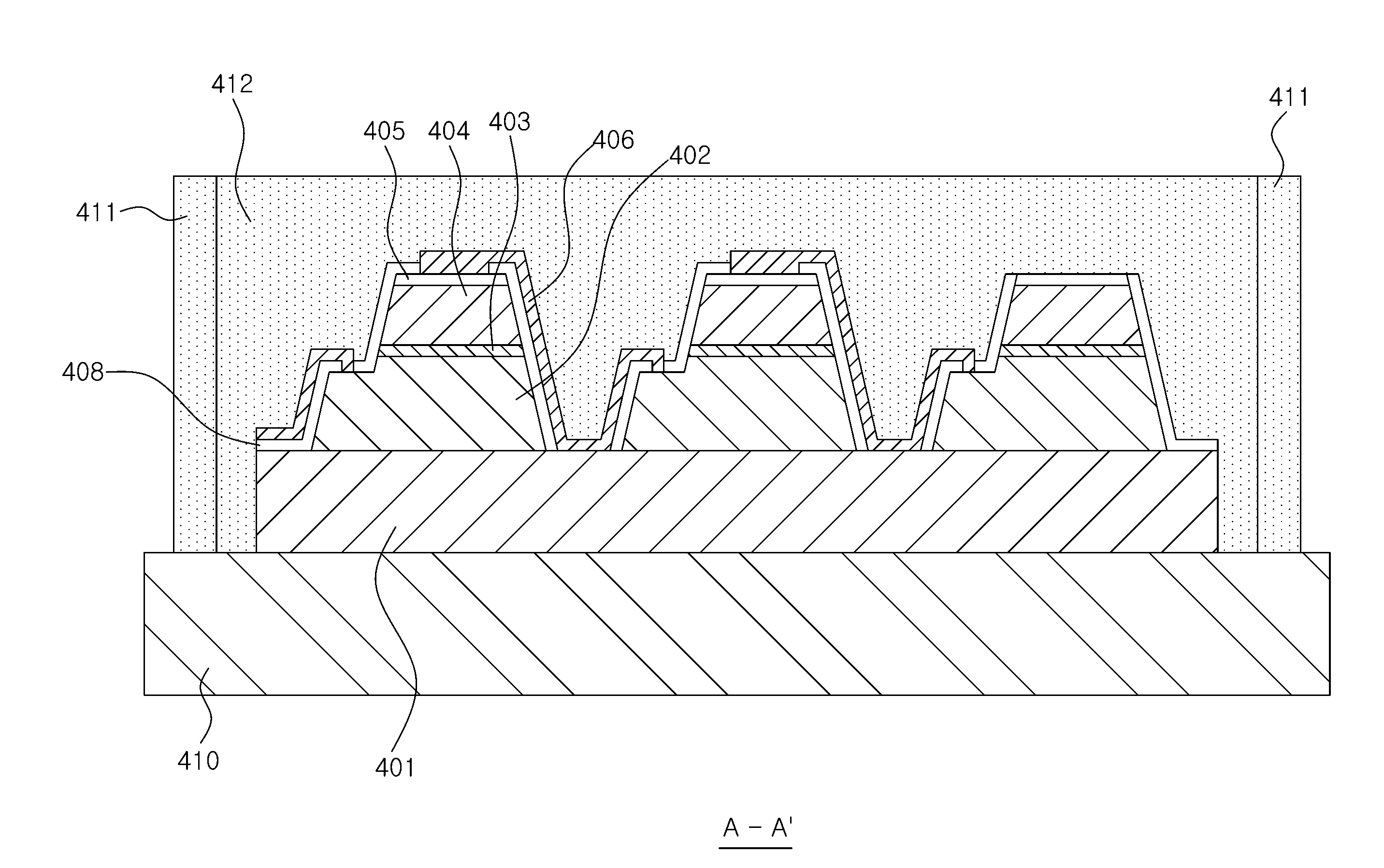
[0081]Exemplary embodiments of the present invention will now be described in detail with reference to the accompanying drawings. The invention may, however, be embodied in many different forms and should not be construed as being limited to the embodiments set forth herein. Rather, these embodiments are provided so that this disclosure will be thorough and complete, and will fully convey the scope of the invention to those skilled in the art. In the drawings, the thicknesses of layers and regions are exaggerated for clarity. Like reference numerals in the drawings denote like elements, and thus their description will be omitted.

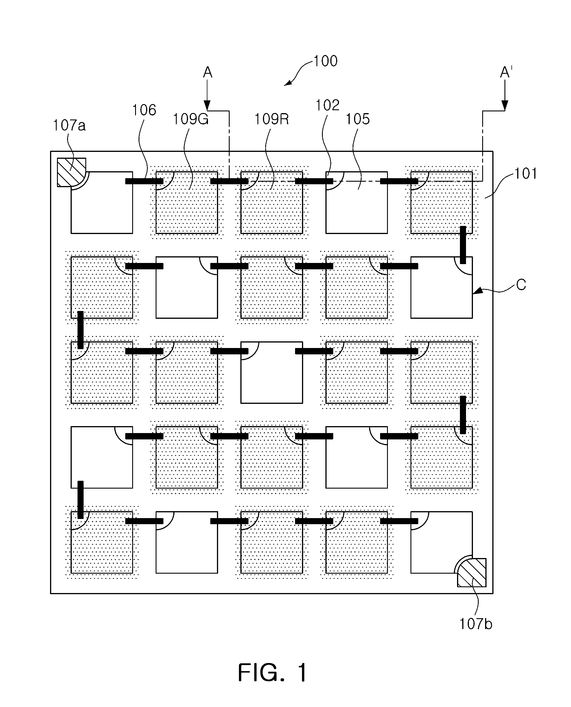
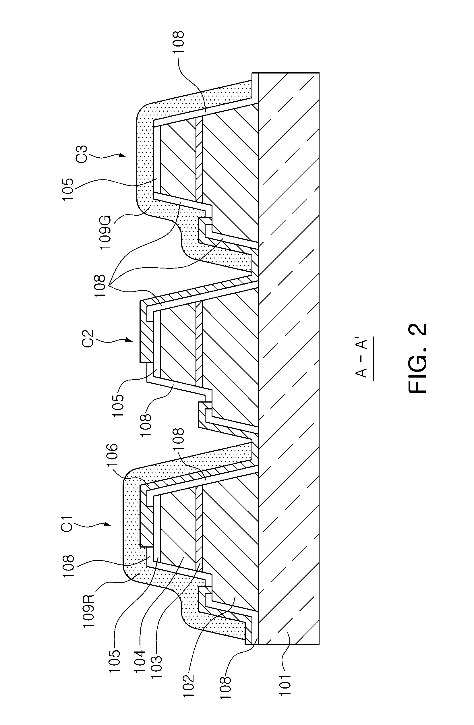
[0082]FIG. 1 is a schematic plan view illustrating a semiconductor light emitting device according to an embodiment of the present invention. FIG. 2 is a schematic cross-sectional view taken along line A-A′ of FIG. 1. FIG. 3 is an equivalent circuit diagram illustrating a connection of light emitting cells in the semiconductor light emitting device of FIG. 1...


PUM


Abstract

A semiconductor light emitting device includes: a substrate; a plurality of light emitting cells arranged on the substrate, each of the light emitting cells including a first-conductivity-type semiconductor layer, a second-conductivity-type semiconductor layer, and an active layer disposed therebetween to emit blue light; an interconnection structure electrically connecting at least one of the first-conductivity-type semiconductor layer and the second-conductivity-type semiconductor layer of the light emitting cell to at least one of the first-conductivity-type semiconductor layer and the second-conductivity-type semiconductor layer of another light emitting cell; and a light conversion part formed in at least a portion of a light emitting region defined by the plurality of light emitting cells, the light conversion part including at least one of a red light conversion part having a red light conversion material and a green light conversion part having a green light conversion material.

Description

CROSS-REFERENCE TO RELATED APPLICATIONS[0001]This application claims the priorities of Korean Patent Application Nos. 2010-0018259 filed on Feb. 26, 2010 and 2010-0085707 filed on Sep. 1, 2010 in the Korean Intellectual Property Office, the disclosure of which is incorporated herein by reference.BACKGROUND OF THE INVENTION[0002]1. Field of the Invention[0003]The present invention relates to a semiconductor light emitting device, and more particularly, to a semiconductor light emitting device, in which a plurality of light emitting cells are arranged, and a method for manufacturing the same.[0004]2. Description of the Related Art[0005]In general, semiconductor light emitting diodes (LEDs) are advantageous for light sources in terms of power, efficiency and reliability. Therefore, semiconductor LEDs are being actively developed as high-power, high-efficiency light sources for various illumination apparatuses as well as for a backlight unit of a display device. For the commercializatio...

Claims


Application Information

Patent Timeline
Patent Type & Authority Applications(United States)
IPC IPC(8): H01L33/08
CPCH01L27/156H01L33/50H01L33/62H01L33/08H01L2924/0002H01L2924/00
Inventor KIM, JE WONJANG, TAE SUNGWOO, JONG GUNLEE, JONG HO
Owner SAMSUNG ELECTRONICS CO LTD
Why Eureka
Try Eureka