Field effect transistor and method of manufacturing the same

a field effect transistor and transistor technology, applied in the direction of basic electric elements, electrical apparatus, semiconductor devices, etc., can solve the problems of drain current decrease, on-resistance increase, channel resistance, on-resistance increase, etc., to reduce on-resistance and increase threshold voltage

Active Publication Date: 2011-09-22
PANASONIC CORP
View PDF17 Cites 44 Cited by
  • Summary
  • Abstract
  • Description
  • Claims
  • Application Information

AI Technical Summary

Benefits of technology

[0012]Now, in view of the above-mentioned problems, it is a first object of the present invention to provide a field effect transistor and a method of manufacturing the field effect transistor that are capable of increasing the threshold voltage as well as decreasing the on-resistance.
[0030]According to this method, when the third nitride semiconductor layer is etched and the surface of the second nitride semiconductor layer is exposed, the second nitride semiconductor layer is not etched. Accordingly, the film thickness of the second nitride semiconductor layer immediately below the gate electrode can be precisely controlled.

Problems solved by technology

In this case, there is a problem in that on-resistance increases because the channel resistances between the gate and source electrodes, and between the gate and drain electrodes increase along with the increase in the threshold voltage (in the positive direction).
In addition, after the above-mentioned JFET is actually fabricated by the inventors, a problem was found that when the gate is turned on immediately after the gate is turned off and a high drain voltage is applied, the drain current decreases and the on-resistance increases, so-called current collapse phenomenon occurs in contrast to the case where the gate is turned on without a high drain voltage being applied.
The increase of the on-resistance due to the current collapse is a serious problem for the power transistor to which a high drain voltage is applied.

Method used


Image

  • Field effect transistor and method of manufacturing the same
  • Field effect transistor and method of manufacturing the same
  • Field effect transistor and method of manufacturing the same

Examples


first embodiment

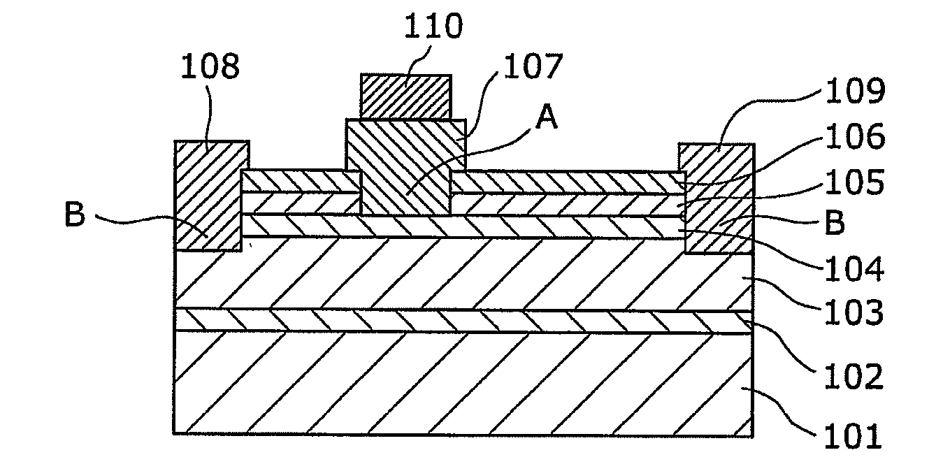
[0044]FIG. 1 is a cross-sectional view showing the structure of a JFET according to a first embodiment of the present invention.

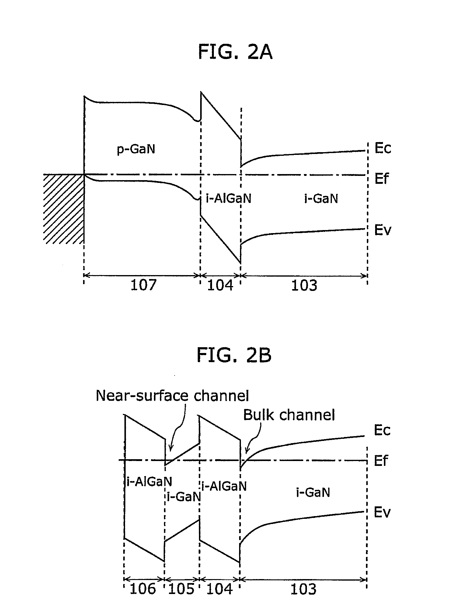
[0045]As shown in the figure, the JFET of the present embodiment is normally-off, and includes 100 nm thick AlN buffer layer 102; 100 nm thick AlN buffer layer 102; 2 μm thick undoped GaN layer 103; 10 nm thick undoped AlGaN layer 104 with 15% of Al composition ratio; 20 nm thick undoped GaN layer 105; 25 nm thick undoped AlGaN layer 106 with 25% of Al composition ratio; and 100 nm thick p-type GaN layer 107 on the (0001) plane of a substrate 101 composed of sapphire. A gate electrode 110 is formed on the p-type GaN layer 107; and a source electrode 108 and a drain electrode 109 are formed in both lateral regions of the gate electrode 110. “Undoped” herein means that an impurity is not intentionally doped.

[0046]In the source and drain regions of the undoped AlGaN layer 104, the undoped GaN layer 105, and the undoped AlGaN layer 106, a recess (B in FIG. 1) i...

second embodiment

[0075]FIG. 5 is a cross-sectional view showing the structure of a JFET according to a second embodiment of the present invention.

[0076]As shown in FIG. 5, the JFET of the present embodiment differs from the JFET of the first embodiment in that the heterojunction interface made between the undoped AlGaN layer 502 and the undoped GaN layer 501 is provided between the gate and source electrodes and between the gate and drain electrodes. Specifically, the JFET of the present embodiment differs from the JFET of the first embodiment in that the undoped GaN layer 501 is provided on the undoped AlGaN layer 106, and the undoped AlGaN layer 502 is provided on the undoped GaN layer 501. Thereby, a near-surface channel is further formed between the gate and source electrodes and between the gate and drain electrodes, thus the channel resistance can be further reduced, and the on-resistance can be further decreased because of the resulting two channels. At this point, the source electrode 108 an...


PUM


Abstract

The present invention has an object to provide an FET and a method of manufacturing the FET that are capable of increasing the threshold voltage as well as decreasing the on-resistance. The FET of the present invention includes a first undoped GaN layer; a first undoped AlGaN layer formed on the first undoped GaN layer, having a band gap energy greater than that of the first undoped GaN layer; a second undoped GaN layer formed on the first undoped AlGaN layer; a second undoped AlGaN layer formed on the second undoped GaN layer, having a band gap energy greater than that of the second undoped GaN layer; a p-type GaN layer formed in the recess of the second undoped AlGaN layer; a gate electrode formed on the p-type GaN layer; and a source electrode and a drain electrode which are formed in both lateral regions of the gate electrode, wherein a channel is formed at the heterojunction interface between the first undoped GaN layer and the first undoped AlGaN layer.

Description

CROSS REFERENCE TO RELATED APPLICATION[0001]This is a continuation application of PCT application No. PCT / JP2009 / 006372 filed on Nov. 26, 2009, designating the United States of America.BACKGROUND OF THE INVENTION[0002](1) Field of the Invention[0003]The present invention relates to a field effect transistor and a method of manufacturing the field effect transistor, and particularly relates to a field effect transistor composed of a group III nitride semiconductor and a method of manufacturing the field effect transistor.[0004](2) Description of the Related Art[0005]In recent years, field effect transistors (FET) as power switching devices using gallium nitride (GaN) based materials have been actively researched. Nitride semiconductor materials such as GaN can be combined with aluminum nitride (AlN) or indium nitride (InN) to form various mixed crystals, and thus can form a heterojunction similarly to the arsenic-based semiconductor material such as conventional gallium arsenide (GaA...

Claims


Application Information

Patent Timeline
Patent Type & Authority Applications(United States)
IPC IPC(8): H01L29/20H01L21/337H01L29/808
CPCH01L29/808H01L29/205H01L29/41766H01L29/2003H01L29/7786H01L29/1066H01L29/66462
Inventor HIKITA, MASAHIROISHIDA, HIDETOSHIUEDA, TETSUZO
Owner PANASONIC CORP
Why Eureka
Try Eureka