Mlc self-raid flash data protection scheme

a self-raid flash and data protection technology, applied in the direction of memory adressing/allocation/relocation, instruments, coding, etc., can solve the problems of long delay between operations, limiting the use of read/write capabilities, and generating unpredictable consequences from power interruptions

Active Publication Date: 2011-09-22
SANDISK TECH LLC
View PDF30 Cites 120 Cited by
  • Summary
  • Abstract
  • Description
  • Claims
  • Application Information

AI Technical Summary

Benefits of technology

[0014]The present invention provides a two-dimensional self-RAID method of protecting, following a power loss, page-based storage data in a multiple-level-cell flash memory device. The process includes reserving a parity sector in each data page under an application of RAID (“First dimensional RAID”) technique, thereby for

Problems solved by technology

The constraints of the head/media technology limit the read/write capabilities to using only one active head at a time.
All data requests that are sent to the drive are handled in a serial manner, with long delays between operations, as the actuator moves the read/write head to the required position and the media rotates to place the data under the read/write head.
As a result, multiple data bits that share the same cell and their electronic states, (hence their threshold voltage Vt's), are interdependent to a point that an unexpected power interruption can generate unpredictable consequences.
In spite of the advantages of MLC over SLC, MLC flash memory devices have not traditionally been used because of certain technical constraints, among which data corruption presents one of the most severe challenges.
MLC flash memory devices are more vulnerable to data corruption than SLC flash memory devices.
The lower cycle limit in the MLC flash memory devices poses particular problems for data centers that operate with unpredictable data streams.
The unpredictable data streams may cause “hot spots”, resulting in certain highly-used areas of memory being subject to a large number of erase cycles.
In addition, various factors in normal operation can also affect flash memory integrity, including read disturbs or program disturbs.
These disturbs lead to unpredictable loss of data bits in a memory cell, as a result of the reading or writing of memory cells adjacent to the disturbed cell.
Sudden data losses in MLC flash memory devices due to unexpected power interruptions require frequent data recoveries.
Because some data levels require more than one write operations to achieve and because more than one bit of data share the same memory cell, a power change or a program error during a write data operation leaves the data in a wrong state.
When the power returns, the memory cell can be in an erratic state.
Therefore a power interruption is a major risk to the integrity of data stored in MLC flash memory devices.
If the power failure occurs while the MLC is in the middle of an operation that changes the contents of

Method used


Image

  • Mlc self-raid flash data protection scheme
  • Mlc self-raid flash data protection scheme
  • Mlc self-raid flash data protection scheme

Examples


Embodiment Construction

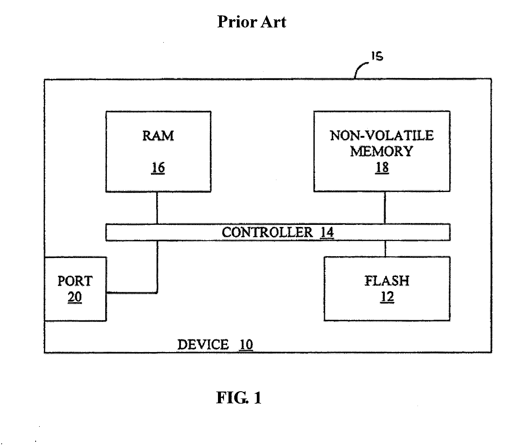
[0039]FIG. 1 is a high level schematic block diagram of a conventional NAND flash media device in a non-volatile data storage unit.

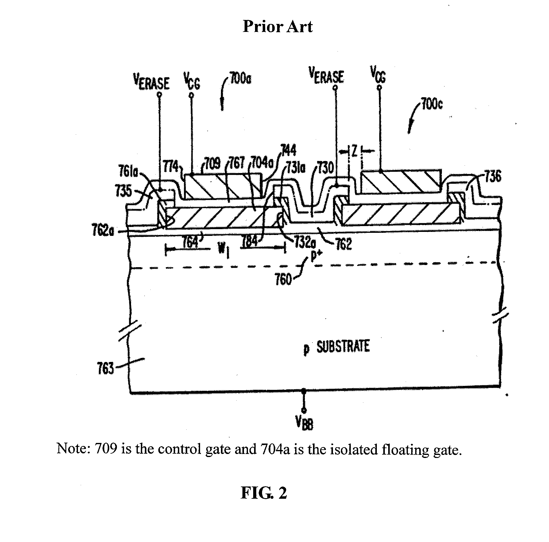
[0040]FIG. 2 shows a cross sectional view of a conventional flash memory device.

[0041]An example of a conventional multiple level (MLC) flash memory cell is illustrated in FIG. 3, where a split channel device has two different threshold voltages, Vt1 and Vt2. The referenced cross sectional view and equivalent circuit are taken from U.S. Pat. No. 5,045,940 (Harari).

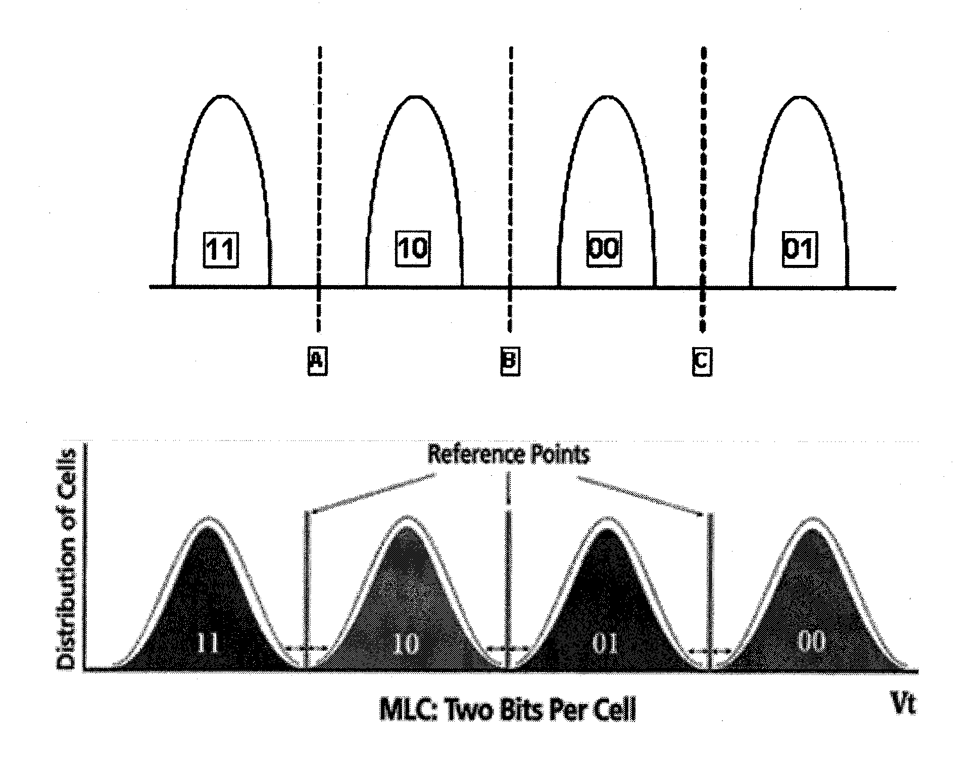
[0042]Variations of the electronic states generate ranges of threshold voltages in a real MLC system. FIG. 4 depicts the threshold voltage spans in a conventional two-bit MLC device.

[0043]Pages of data sharing the same multiple level cells are called “shared pages”. Each manufacturer may use a different distance between its shared pages. Many memory vendors prefer to set the distance at four. For example, at a pair distance of 4, page 0 is paired with page 4, page 1 is paired with page 5, page ...


PUM


Abstract

A two-dimensional self-RAID method of protecting page-based storage data in a MLC multiple-level-cell flash memory device. The protection scheme includes reserving one parity sector across each data page, reserving one parity page as the column parity, selecting a specific number of pages to form a parity group, writing into the parity page a group parity value for data stored in the pages of the parity group. The parity sector represents applying a RAID technique in a first dimension. The group parity represents applying a RAID technique in a second dimension. Data protection is achieved because a corrupted data sector can likely be recovered by the two dimensional RAID data.

Description

CROSS-REFERENCE TO RELATED APPLICATIONS[0001]The present application relates to subject matter in the following copending patent applications: U.S. patent application Ser. No. M-17228-01 US, filed on Apr. 8, 2008, entitled “System and Method for Performing Host Initiated Mass Storage Commands Using a Hierarchy of Data Structures”; U.S. patent application Ser. No. M-17228-02 US, filed on Apr. 8, 2008, entitled “Flash Memory Controller Having Reduced Pinout”; U.S. patent application Ser. No. M-17228-03 US, filed on Apr. 8, 2008, entitled “Multiprocessor Storage Controller”; U.S. patent application Ser. No. M-17228-04 US, filed on Apr. 8, 2008, entitled “Storage Controller for Flash Memory Including a Crossbar Switch Connecting a Plurality of Processors With a Plurality of Internal Memories”; U.S. patent application Ser. No. M-17228-05 US, filed on Apr. 8, 2008, entitled “Flash Memory Controller and System Including Data Pipelines Incorporating Multiple Buffers”; U.S. patent applicatio...

Claims


Application Information

Patent Timeline
IPC IPC(8): G11C16/04
CPCG06F11/1044G11C16/22G06F11/1072G06F11/1012G06F12/02G06F12/16
Inventor OLBRICH, AARON K.PRINS, DOUG
Owner SANDISK TECH LLC
Why Eureka
Try Eureka