

Method for manufacturing 3-dimensional structures using thin film with columnar NANO pores and manufacture thereof
- Summary
- Abstract
- Description
- Claims
- Application Information
AI Technical Summary
Benefits of technology
Problems solved by technology
Method used
Image

Examples
Embodiment Construction
[0064][A Method for Forming a Device]
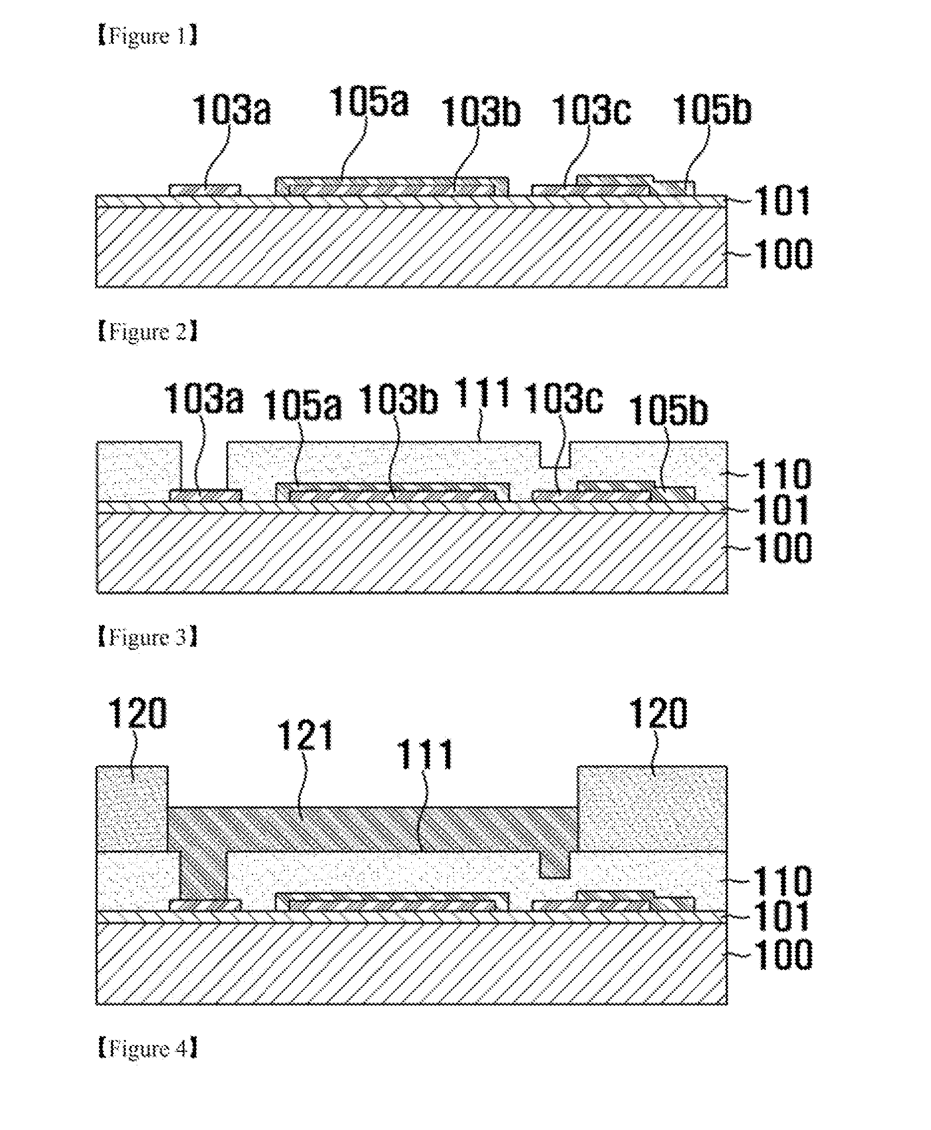
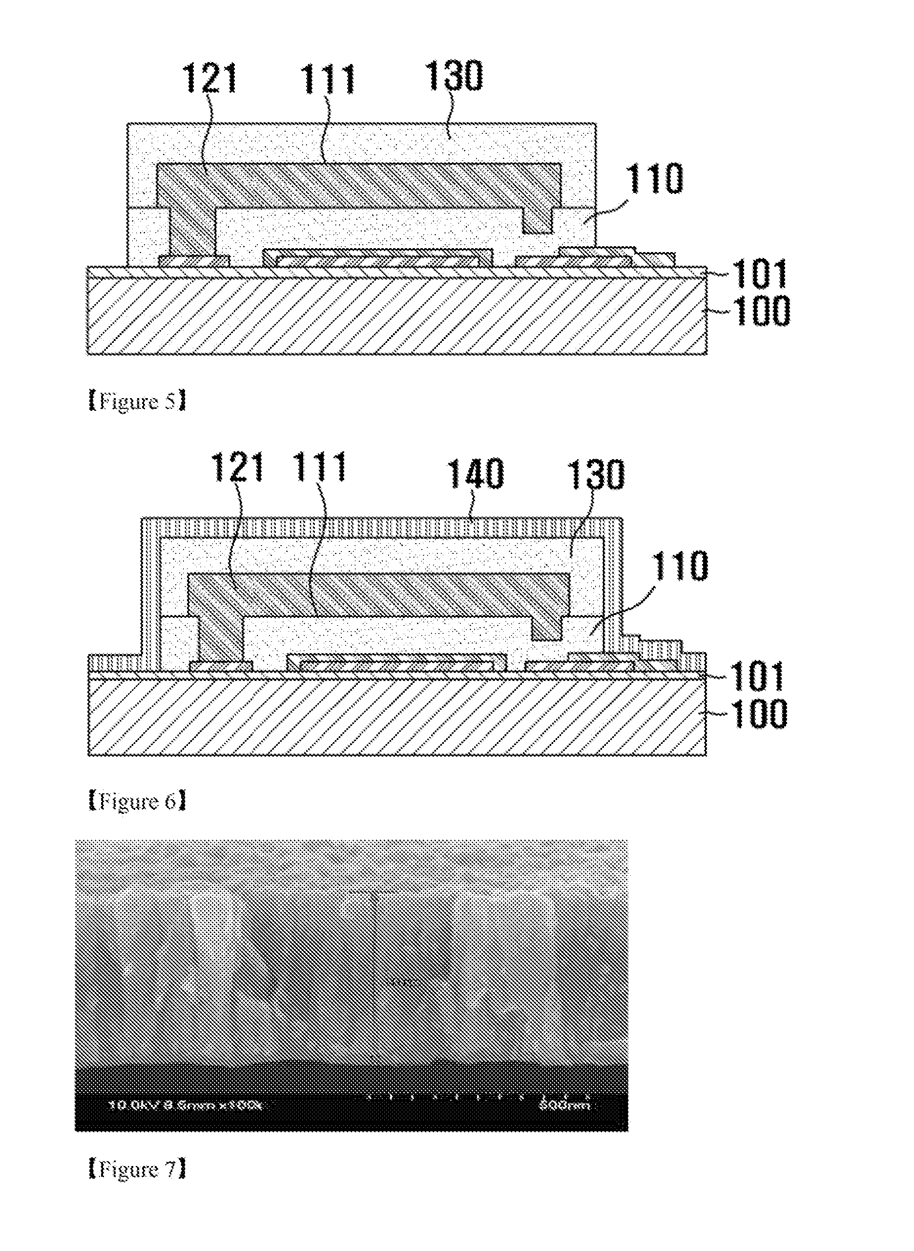
[0065]Prior to a detailed description of a method for packaging an device, a method for forming an device according to an embodiment of the present invention will be described. Particularly, a detailed description of the method for forming the device will be given taking an example of a method for forming an MEMS switch device or an NEMS switch device.
[0066]FIGS. 1 to 3 show a method for forming an MEMS switch device or an NEMS switch device according to the present invention.
[0067]First, as shown in FIG. 1, a first insulation layer 101 is formed on a substrate 100. The substrate 100 includes a silicon substrate, a glass substrate or a plastic substrate. The first insulation layer 101 is formed by one of a low pressure chemical vapor deposition (LPCVD), plasma enhanced chemical vapor deposition (PECVD) and atmospheric pressure chemical vapor deposition (APCVD). Then, metal electrodes 103a, 103b and 103c of the switch device and second insulation ...
PUM
 Abstract
Description
Claims
Application Information