Copper alloy and electrically conductive material for connecting parts, and mating-type connecting part and method for producing the same

a technology of copper alloy and electrically conductive material, which is applied in the manufacture of contact parts, superimposed coating processes, transportation and packaging, etc., can solve problems such as solder wettability problems, and achieve the effects of low insertion force, excellent electrical reliability, and low insertion for

Inactive Publication Date: 2011-09-29
KOBE STEEL LTD +1
View PDF5 Cites 24 Cited by
  • Summary
  • Abstract
  • Description
  • Claims
  • Application Information

AI Technical Summary

Benefits of technology

[0038]The present invention provides an electrically conductive material for connecting parts, which achieves low insertion force in response to the miniaturization of terminals and has excellent electrical reliability.
[0039]The present invention also provides a mating-type connecting part that achieves low insertion for...

Problems solved by technology

At the mating portion, the Cu—Sn alloy layer and the Sn layer are formed on the outermost surface (the C...

Method used


Image

  • Copper alloy and electrically conductive material for connecting parts, and mating-type connecting part and method for producing the same
  • Copper alloy and electrically conductive material for connecting parts, and mating-type connecting part and method for producing the same
  • Copper alloy and electrically conductive material for connecting parts, and mating-type connecting part and method for producing the same

Examples


example 1

Production of Cu Alloy Base Material

[0116]In this example, a copper alloy strip containing Ni, Si, Zn, and Sn in amounts of 1.8 mass %, 0.40 mass %, 1.1 mass %, and 0.10 mass % based on Cu, respectively, and having a Vickers hardness of 180 and a thickness of 0.25 mmt was produced.

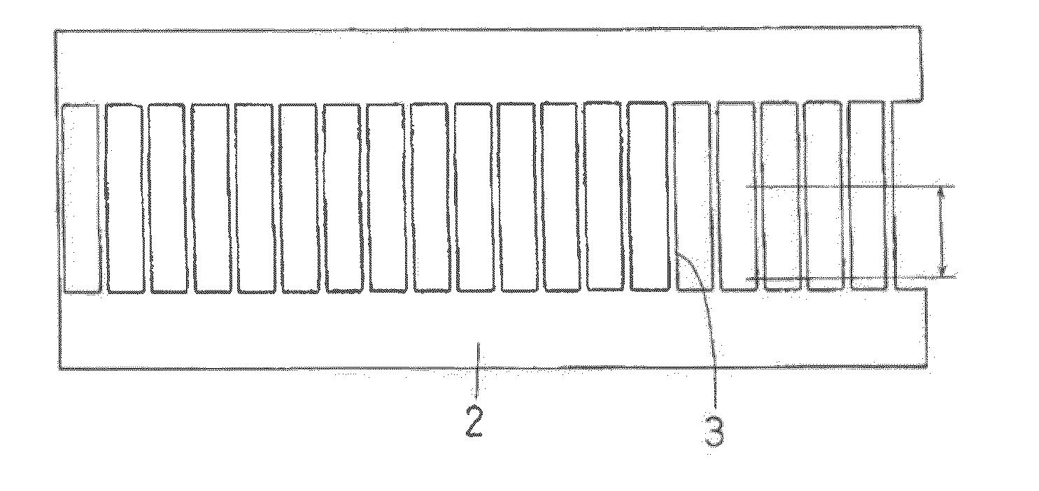
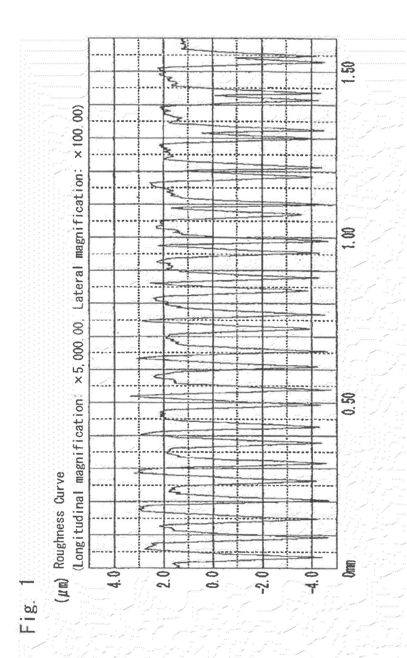
[0117]A specimen with a size of 100 mm×40 mm (rolling / longitudinal direction x perpendicular direction) was cut from the copper alloy strip. A part provided with predetermined depressions and projections on the pressing surface thereof was mounted at a predetermined position in a progressive die for forming pin terminals (position after the formation of the pin terminals), and pin terminal shapes with a size of 1 mm w×22 mm L were formed with a pitch of 5 mm. At the same time, a 1 mm w×10 mm L area of the surface of each pin terminal was surface-roughened. FIG. 5 shows a schematic diagram of the copper sheet after the formation and the surface roughening. In FIG. 5, 2 is the copper sheet, 3 is the pin term...

example 2

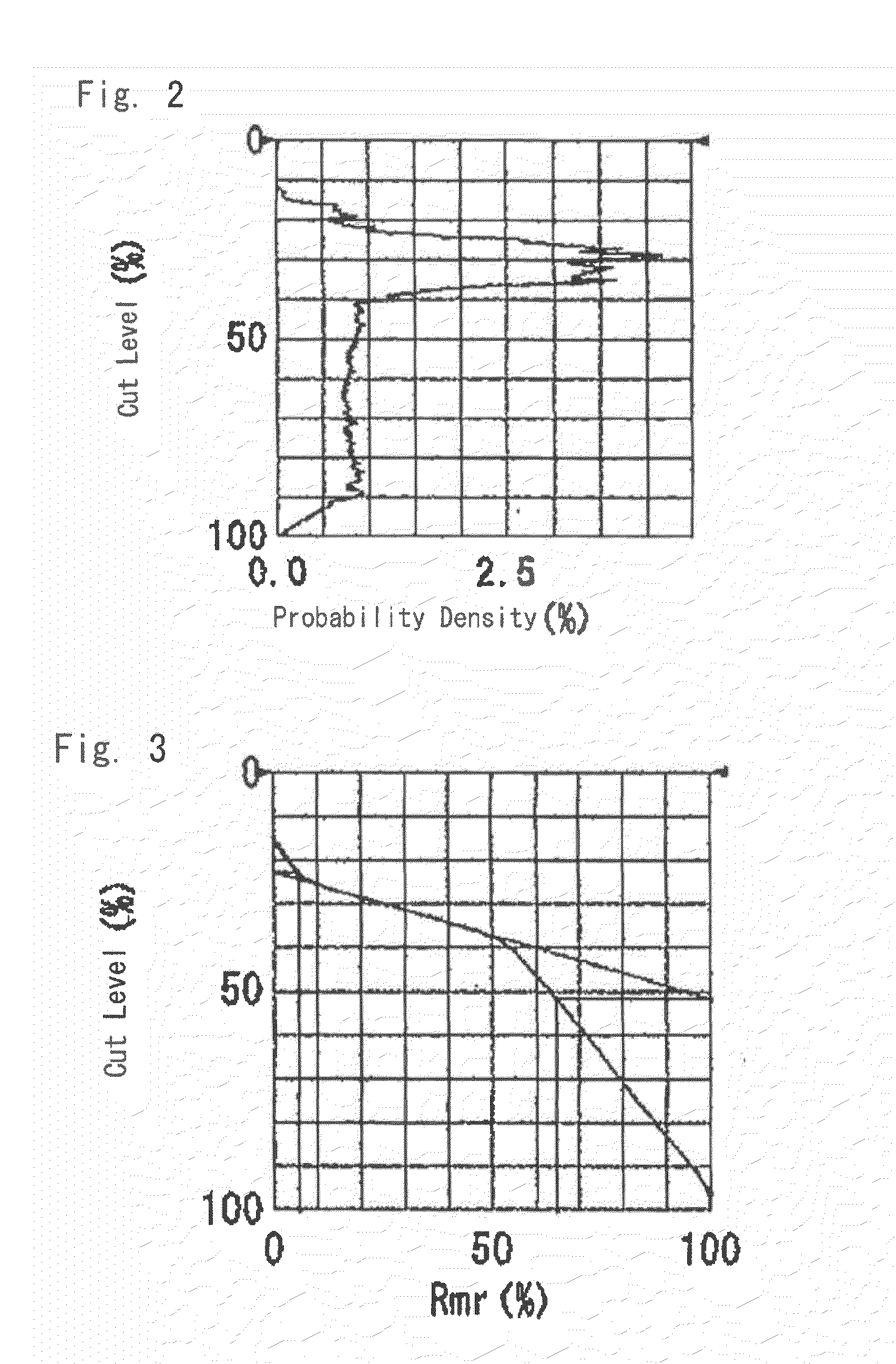
[0132]In addition to Nos. 4, 5, 7, 13, and 14 used in Example 1, No. 17 was newly formed, surface-roughened, plated, and reflowed in the same manner as in Example 1 to prepare specimens. Subsequently, the surface roughness (including protrusion valley portion depth Rvk), the thickness of the Sn coating layer, and the friction coefficient were measured in the same manner. Nos. 4 and 17, as well as Nos. 5 and 14, are similar to each other in terms of arithmetic mean roughness Ra, mean projection-depression interval RSm, skewness Rsk, and protrusion peak portion height Rpk, and are different from each other in terms of protrusion valley portion depth Rvk. Further, Nos. 4, 5, 7, 13, 14, and 17 were measured for contact resistance after high-temperature storage as follows. The results are shown in Table 2.

Contact Resistance Evaluation Test after High-Temperature Storage

[0133]Each test material was heat-treated in air at 160° C. for 120 hours and 500 hours, and then measured for contact r...

example 3

Production of Copper Plate Material (Plated Base Material)

[0136]In this example, as in the paragraph [0060], a copper alloy strip containing Ni, Si, Zn, and Sn in amounts of 1.8 mass %, 0.40 mass %, 1.1 mass %, and 0.10 mass % based on Cu, respectively, and having a Vickers hardness of 180 and a thickness of 0.25 mmt was produced.

[0137]A specimen with a size of 100 mm×40 mm (rolling / longitudinal direction×perpendicular direction) was cut from the copper alloy strip. A part provided with predetermined depressions and projections on the pressing surface thereof was mounted at a predetermined position in a progressive die for forming pin terminals (position after the formation of the pin terminals), and pin terminal shapes with a size of 1 mm w×22 mm L were formed with a pitch of 5 mm. At the same time, a 1 mm w×10 mm L area of the surface of each pin terminal was surface-roughened. FIG. 12 shows a schematic diagram of the copper sheet after the terminal formation and the surface rough...


PUM

PropertyMeasurementUnit
Lengthaaaaaaaaaa
Lengthaaaaaaaaaa
Lengthaaaaaaaaaa

Abstract

The surface roughness of a copper sheet is adjusted to have an arithmetic mean roughness Ra of 0.5 μm or more and 4.0 μm or less in a direction parallel to a sliding direction upon connection, a mean projection-depression interval RSm of 0.01 mm or more and 0.3 mm or less in the direction, a skewness Rsk of less than 0, and a protrusion peak portion height Rpk of 1 μm or less. Further, as a surface coating layer, a Sn coating layer group X observed as a plurality of parallel lines is included, and a Cu—Sn alloy coating layer is present adjacent to each side of each of Sn coating layers constituting the Sn coating layer group X. The maximum height roughness Rz is 10 μm or less in a direction of part insertion. At the time of stamping the copper sheet, the copper sheet is surface-roughened by pressing, thereby forming depressions observed as a plurality of parallel lines in the surface of the copper sheet. The copper sheet is then plated with Cu and Sn, followed by reflowing to complete the production.

Description

BACKGROUND OF THE INVENTION[0001]1. Field of the Invention[0002]The present invention relates to an electrically conductive material for connecting parts, such as a terminal for connectors or a bus bar used mainly for electrical wiring in automobiles, household equipment, and the like, and also to a mating-type connecting part and a method for producing the same. The present invention particularly relates to an electrically conductive material for connecting parts and a mating-type connecting part, which are expected to have both reduced friction or abrasion upon the insertion and extraction of male and female terminals and electrical connection reliability in use, and a method for producing the same.[0003]2. Description of the Related Art[0004]JP-B-3926355 describes an electrically conductive material for connecting parts, which has high electrical reliability (low contact resistance) and a low friction coefficient and is suitable as a terminal for a mating-type connector. Accordin...

Claims


Application Information

Patent Timeline
IPC IPC(8): B32B3/30B32B15/01H01R43/16H01R43/00
CPCC23C28/021C25D5/10C25D5/12C25D5/34C25D5/50C25D5/505Y10T428/12708Y10T428/12389H01R43/16B32B15/00Y10T29/49206Y10T29/49224Y10T29/49204H01R13/03C25D5/605Y10T428/12715Y10T428/12722Y10T428/12861Y10T428/12903
Inventor MASAGO, YASUSHITAIRA, KOICHIMITSUI, TOSHIYUKIKAKUMOTO, JUNICHI
Owner KOBE STEEL LTD
Why Eureka
Try Eureka