Method of manufacturing semiconductor device

a manufacturing method and semiconductor technology, applied in semiconductor devices, semiconductor/solid-state device details, electrical devices, etc., can solve the problems of difficult to fabricate highly reliable semiconductor devices, reduce the size of the overall semiconductor device, and cracks in the filling material, so as to reduce the overflow width, prevent cavities, and improve the reliability of semiconductor devices

Inactive Publication Date: 2011-10-06
LONGITUDE SEMICON S A R L
View PDF2 Cites 22 Cited by
  • Summary
  • Abstract
  • Description
  • Claims
  • Application Information

AI Technical Summary

Benefits of technology

According to the method of manufacturing a semiconductor device of the present invention mentioned above, in filling the resin material in the spaces between the stacked semiconductor chips, a supercritical film deposition process is applied. In the supercritical film deposition process, the resin material is mixed in the supercritical fluid, the resin material is caused to flow into the spaces between the semiconductor chips, and the resin material is polymerized on the surfaces between the plurality of the semiconductor chips, so that the spaces between the stacked semiconductor chips are sufficiently filled with the resin material. Therefore, according to the present invention, the resin material is sufficiently filled between the plurality of the semiconductor chips. Accordingly, it is possible to prevent cavities from being produced between the plurality of the semiconductor chips.
In addition, the polymerization reaction of the resin material takes place almost simultaneously between the individual semiconductor chips, from the surfaces of the individual semiconductor chips vertically upward. As a result, the overflow, which is formed by the resin filling material running in a direction orthogonal to the stacking direction of the semiconductor chips (the height direction of the stacked unit) from the side surfaces of the stacked unit, is formed have a shape such that it follows the side surfaces of each semiconductor chip. Consequently, it is possible to prevent the overflow from forming in a tapered shape in which the overflow becomes wider vertically downward along the stacked unit. Accordingly, according to the present invention, it is possible to reduce the overflow width.
According to the present invention, in order to improve the reliability of semiconductor devices, it is possible to prevent voids or cracks from being produced in a resin material between semiconductor chips. In addition, according to the present invention, in order to reduce the size of semiconductor devices, it is possible to prevent a resin material that fills the spaces between semiconductor chips from running in a direction that is orthogonal to the stacking direction of the semiconductor chips.

Problems solved by technology

In the case in which voids remain between the stacked semiconductor chips, it is likely that the under-fill material cracks when heated and cooled in the semiconductor device manufacturing processes after the stacking process.
More specifically, in the filling method in which the under-fill material is caused to flow between the semiconductor chips using the above-mentioned capillary actions, it is difficult to fabricate highly reliable semiconductor devices because the spaces, which are narrowed between the vertically stacked semiconductor chips with the development of high integration, cannot be completely filled.
Therefore, the overflow width is a factor that hampers a reduction in the size of the overall semiconductor device.
However, the method proposed in JP2007-036184β is not applicable to the case of stacking a plurality of semiconductor chips having the same outside dimensions.

Method used


Image

  • Method of manufacturing semiconductor device
  • Method of manufacturing semiconductor device
  • Method of manufacturing semiconductor device

Examples


first embodiment

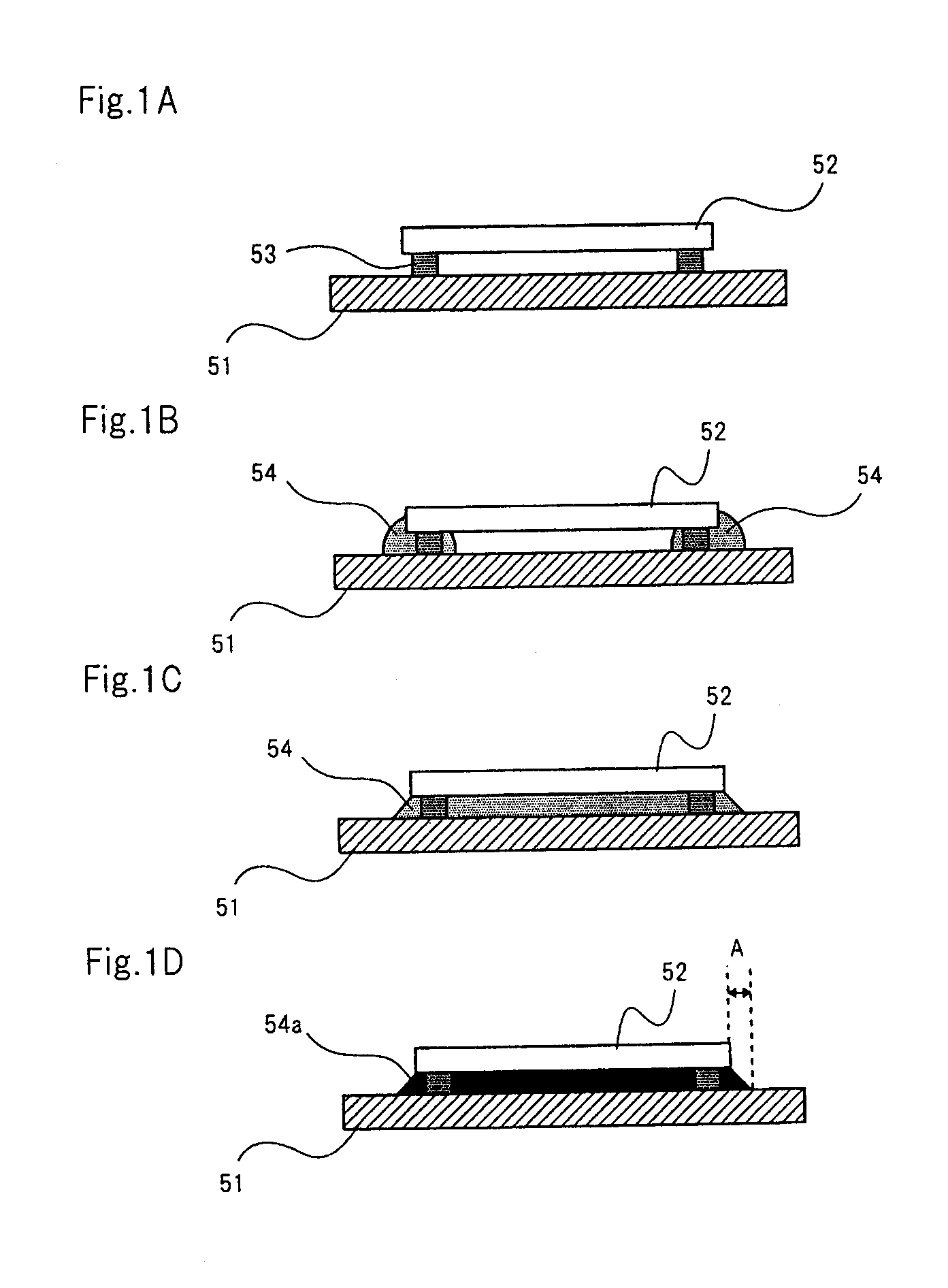
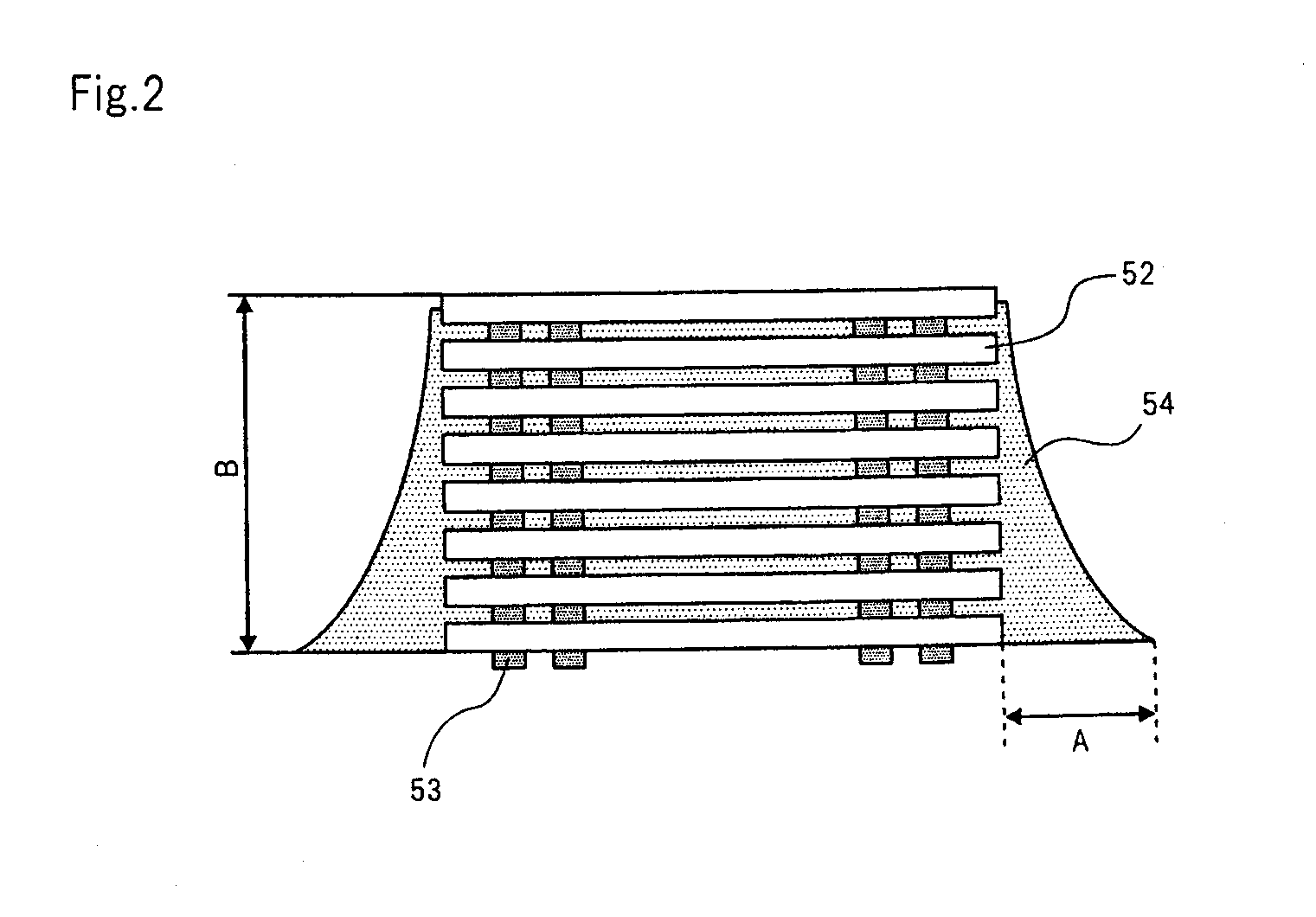
In a method of manufacturing a semiconductor device according to this embodiment, a resin material is filled in the spaces between stacked semiconductor chips using a film deposition process in a supercritical state. Here, a supercritical state refers to a state in which the pressure and temperature to be applied to a substance are at and beyond a value (critical point) specific to this substance to cause the substance to have characteristics of both gas and liquid.

FIG. 3 shows a schematic diagram depicting a supercritical apparatus used for the method of manufacturing a semiconductor device according to the first embodiment. FIG. 4 shows a schematic plan view depicting heater 9 included in the high-pressure vessel of the supercritical apparatus.

As shown in FIG. 3, the supercritical apparatus used for the method of manufacturing a semiconductor device comprises high-pressure vessel 7 in which stacked unit 30 having a plurality of stacked semiconductor chips is placed as a processing...

second embodiment

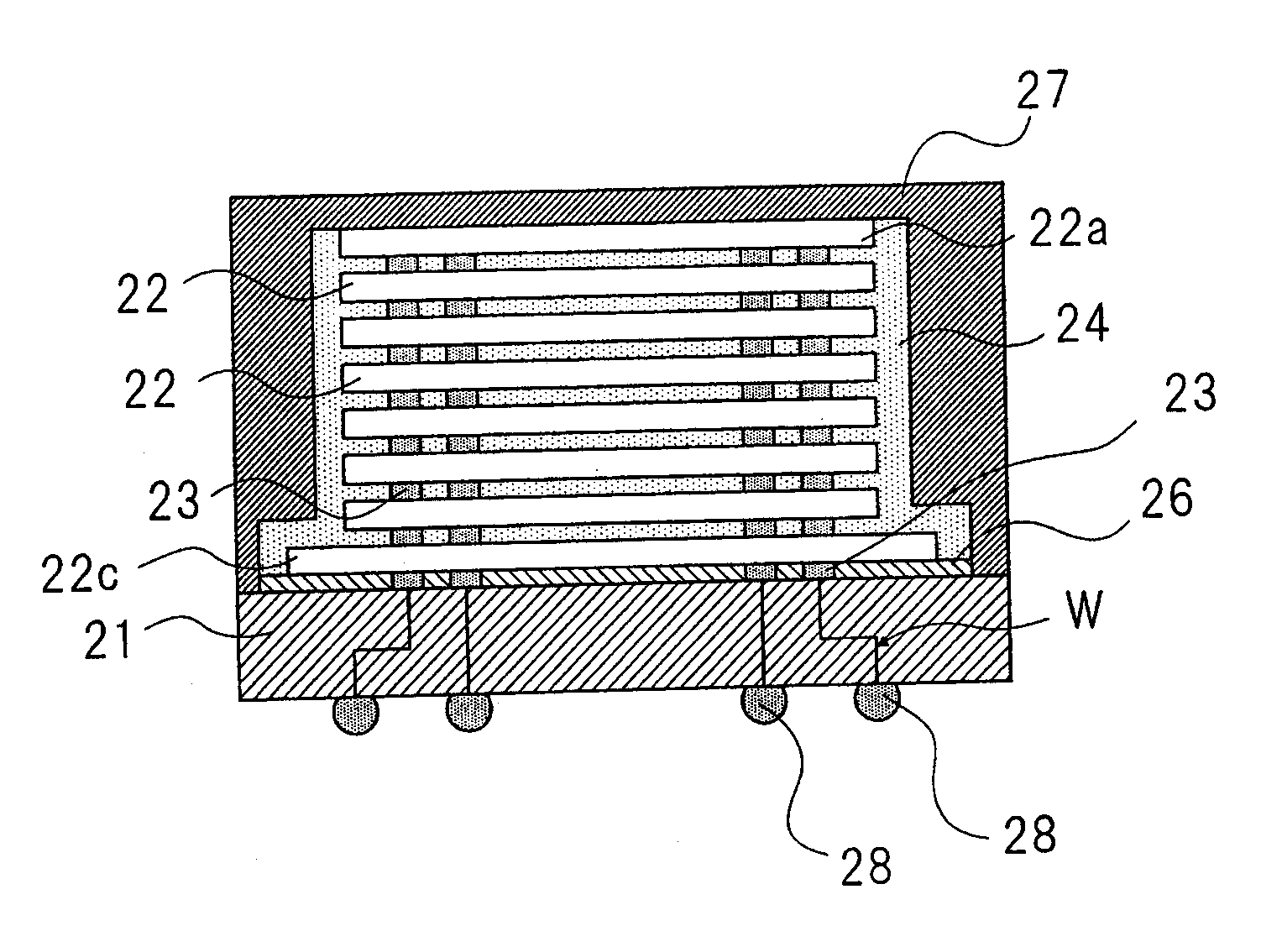
Next, an exemplary structure in which the outside dimensions of semiconductor chips that are to be stacked are different will be described with reference to the drawings. FIG. 10 is a vertical cross sectional view depicting a stacked unit used in a method of manufacturing a semiconductor device according to a second embodiment. FIG. 11 is a vertical cross sectional view illustrative of the method of manufacturing a semiconductor device according to the second embodiment. FIG. 12 is a vertical cross sectional view depicting a semiconductor device fabricated by the method of manufacturing a semiconductor device according to the second embodiment. In addition, in the second embodiment, the same components as those in the first embodiment are designated the same numerals and signs that are in the first embodiment, and the description is omitted.

As shown in FIG. 10, stacked unit 31 is prepared, in which only the outside dimensions of lowermost semiconductor chip 22c are greater than the ...


PUM


Abstract

A method of manufacturing a semiconductor device includes: supplying a supercritical fluid mixed with an under-fill material to a stacked unit, which has a plurality of stacked semiconductor chips; and filling the under-fill material in the space between the plurality of the semiconductor chips, by heating the stacked unit placed in the inside of the high-pressure vessel and curing the under-fill material flowing in the space between the plurality of the semiconductor chips by a polymerization reaction, while the supercritical fluid is being supplied.

Description

BACKGROUND OF THE INVENTION1. Field of the InventionThe present invention relates to a method of manufacturing a semiconductor device having a plurality of stacked semiconductor chips.2. Description of the Related ArtTo meet demands for a reduction in the size of semiconductor devices, COC (Chip On Chip) techniques are known in which a plurality of semiconductor chips are stacked and mounted on a single semiconductor device (semiconductor package). COC semiconductor devices are disclosed in JP2005-142210A, JP2005-032820A, and JP2007-036184A.More particularly, such a structure is known in which a plurality of semiconductor chips are stacked in such a way that bump electrodes are disposed on the top and under sides of semiconductor chips and through-vias are used to electrically connect the bump electrodes to circuit elements inside the semiconductor chips. According to this structure, semiconductor devices with a higher integration degree can be implemented, as compared with conventi...

Claims


Application Information

Patent Timeline
Patent Type & Authority Applications(United States)
IPC IPC(8): H01L21/58H01L21/56
CPCH01L21/565H01L21/568H01L21/67017H01L21/67126H01L23/3128H01L23/3135H01L21/561H01L2224/73104H01L2224/81191H01L2224/83191H01L2224/13099H01L2224/83104H01L2924/00014H01L2224/29011
Inventor ODE, HIROYUKIIKEDA, HIROAKI
Owner LONGITUDE SEMICON S A R L
Why Eureka
Try Eureka