Method for producing liquid crystal display apparatus

a liquid crystal display and production method technology, applied in the direction of photomechanical equipment, identification means, instruments, etc., can solve the problems of increasing the production cost of the apparatus, and high unit cost, so as to prevent the reduction of the surface roughness of the rough surface formed by the protrusions and recesses

Inactive Publication Date: 2005-04-19
NEC LCD TECH CORP
View PDF6 Cites 30 Cited by
  • Summary
  • Abstract
  • Description
  • Claims
  • Application Information

AI Technical Summary

Benefits of technology

[0022]In the conventional method for manufacturing the active matrix substrate, shown in FIGS. 81 and 82, there are required seven photolithography (PR) processes, namely, a PR process for forming a gate bus wiring and a gate electrode, a PR process for forming a contact layer and a semiconductor layer, a PR process for forming a source electrode, a drain electrode and a source / bus wiring, a PR process for forming the contact hole in the organic insulating film, a PR process for forming the rough surface of the organic insulating film, a PR process for forming the reflective plate and a PR process for forming the transparent electrode. These PR processes lead to increased production cost of the apparatus and hence to a high unit cost.
[0023]In light of the above, it has been desired to lower production cost through reduction in the number of PR steps and to realize high brightness and high quality display performance to enable the high brightness liquid crystal display apparatus at a low cost.
[0024]Accordingly, it is an object of the present invention to provide a liquid crystal display apparatus and a method for producing it, in which an optimum display performance of the liquid crystal display apparatus may be demonstrated even though the number of PR processes is diminished.
[0031]In the method for producing a liquid crystal display apparatus, in accordance with the present invention, the reflector formed in the second step is directly arranged on the rough surface formed by the protrusions and recesses. It is because surface roughness of the rough surface formed by the protrusions and recesses can be prevented from being decreased.
[0032]In the method for producing a liquid crystal display apparatus, in accordance with the present invention, the reflector is of a laminated structure comprised of a lower Cr layer and an upper Al / Nd layer. The source electrode and the drain electrode of the laminated structure are selectively formed when the reflector is formed in the fifth step. A contact hole for partially exposing the Cr layer of the source electrode is formed in an other insulation layer formed on the insulating layer comprised of the reflector, source electrode and the drain electrode, and in the Al / Nd layer, after forming the other insulating layer. A transparent electrode layer electrically connecting to the source electrode through the contact hole is selectively formed on the other insulating layer. It is because optimum electrical conductivity may be maintained between the source electrode and the transparent electrode layer, such as ITO, as hillocks are prevented from being produced on the surface of the Al / Nd layer in the reflector.
[0035]In accordance with a sixth aspect of the present invention, there is provided a method for producing a liquid crystal display apparatus having a first substrate including a thin film transistor and a reflector on an insulating substrate, a second substrate having a transparent electrode and mounted facing the first substrate, and a liquid crystal layer placed between the first substrate and the second substrate, in which the method includes a first step of forming a first metal layer on the insulating substrate and subsequently etching the first metal layer using a first etching mask, to expose a portion of the insulating substrate, and to form a gate electrode, a plurality of protrusions separated therefrom, and a wiring isolated from the gate electrode and the protrusions, a second step of causing only the first etching mask to reflow to cover exposed surfaces of the gate electrode and the wiring and near-by surface portions of the insulating substrate with the first etching mask and to cover exposed surfaces of the protrusions and near-by surface portions of the insulating substrate with the first etching mask, a third step of etching the insulating substrate, using the first etching mask, after the second step, to form one or more recesses in the exposed area of the insulating substrate, a fourth step of etching the semiconductor layer, using a second etching mask, after forming a first insulating film and a semiconductor layer on the insulating substrate, including the gate electrode, the protrusions and the wiring, to form an island above the gate electrode, a fifth step of etching the first insulating layer, using a third etching mask, to expose a portion of the wiring to form a first contact hole, a sixth step of etching a second metal layer, using a fourth etching mask, after forming the second metal layer on the first insulating layer, including the island, to form a source electrode, a drain electrode and a reflector, to electrically connect the source electrode through the first contact hole with the wiring, a seventh step of forming, after forming a second insulating layer on the first insulating layer including the source electrode, drain electrode and the reflector, a second contact hole in the second insulating layer and in the first insulating layer, using a fifth etching mask, for exposing a portion of the wiring, and an eighth step of selectively forming a transparent electrode layer on the second insulating layer for electrically connecting to the wiring through the second contact hole. It is because it is possible to prevent the electrical field applied to the liquid crystal from being reduced when the transparent electrode is in the uppermost layer, and because the source electrode and the transparent electrode can be electrically interconnected through ha wiring to prevent shorting across the drain electrode and the transparent electrode.

Problems solved by technology

In order to produce a liquid crystal display apparatus that is able to make bright high-quality display by using the conventional production method, it is necessary to form high performance transistors and high performance reflectors on one and the same insulating substrate, with the result that a large number of deposition processes, photolithography processes and etching processes are required.
These PR processes lead to increased production cost of the apparatus and hence to a high unit cost.

Method used


Image

  • Method for producing liquid crystal display apparatus
  • Method for producing liquid crystal display apparatus
  • Method for producing liquid crystal display apparatus

Examples


first embodiment

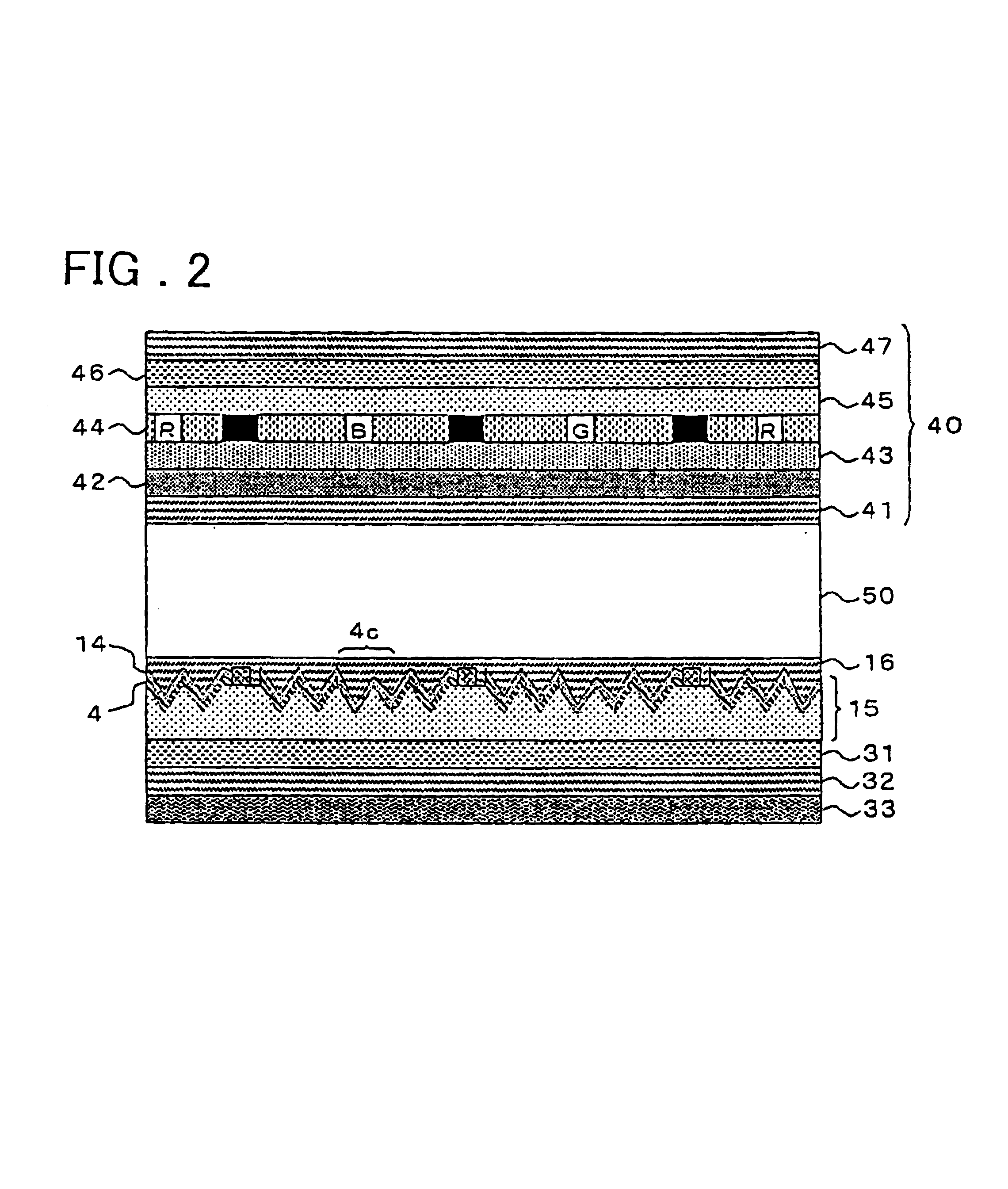
[0145]The process for producing the active matrix substrate is now explained.

[0146]First referring to FIGS. 5, 11a, 12a, 13a, 14a and 15a, a first mask, not shown, is formed on a planar insulating substrate 1 of, for example, glass, by a photolithography technique. A rough surface 1a then is formed on the insulating substrate 1 having a flat surface, such as a glass substrate, by a photolithography technique. Then, by e.g., wet etching, employing HF (hydrofluoric acid), sand-blasting, or dry etching, employing CF4 or O2, a rough surface 1a is formed in a preset area of the insulating substrate 1. The resulting product is washed and the first mask is removed.

[0147]The wet etching of the glass substrate is meritorious in that the back surface of the substrate is simultaneously etched to thereby reduce the substrate thickness.

[0148]Then, referring to FIGS. 6, 11b, 12b, 13b, 14b and 15b, underlying metal layers 2a, 3a, 4a and 17a of, for example, Cr, Ti or Mo (referred to below as ‘Cr’...

second embodiment

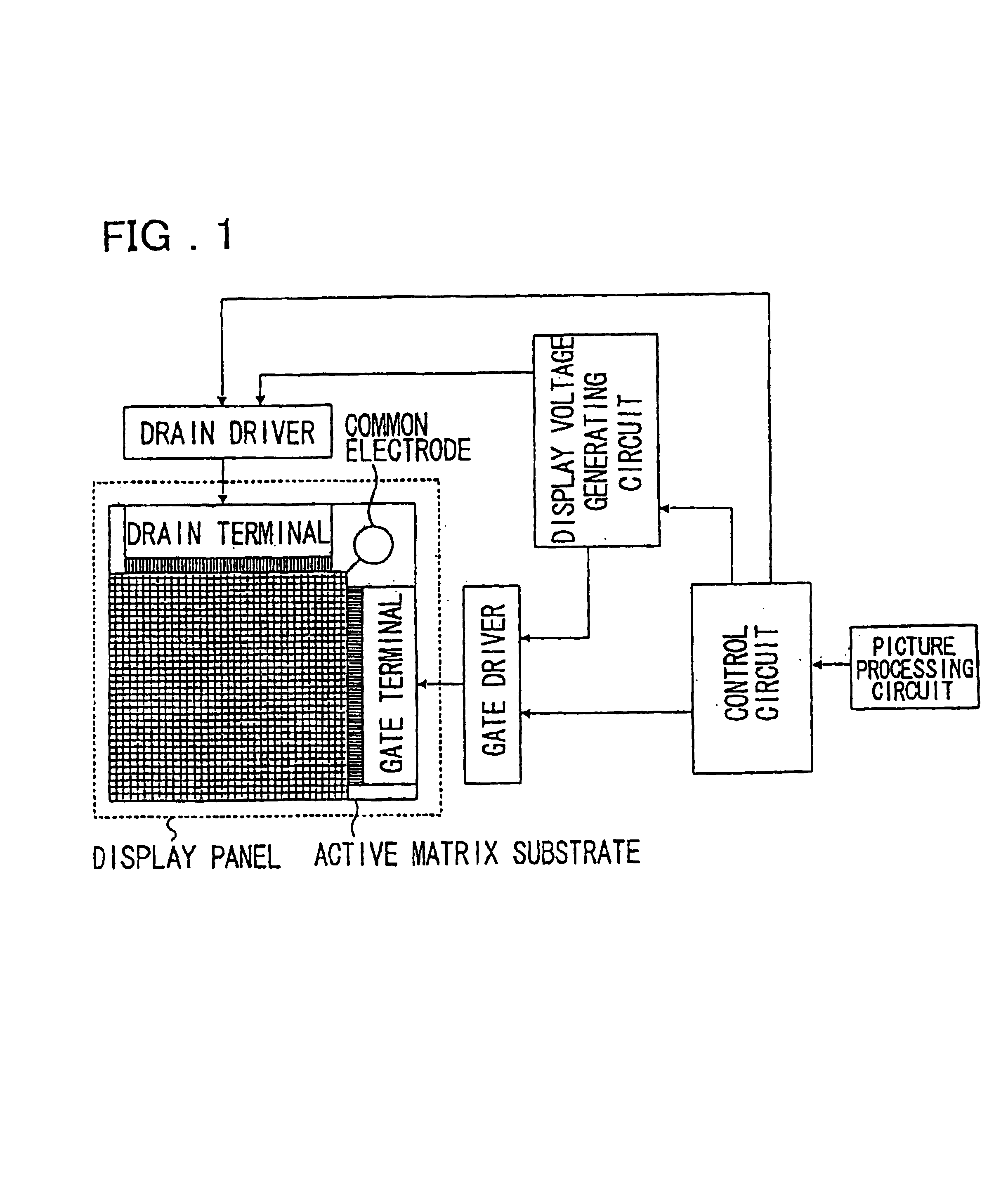
[0179]The production process for the active matrix substrate 15 in the liquid crystal display apparatus is now explained.

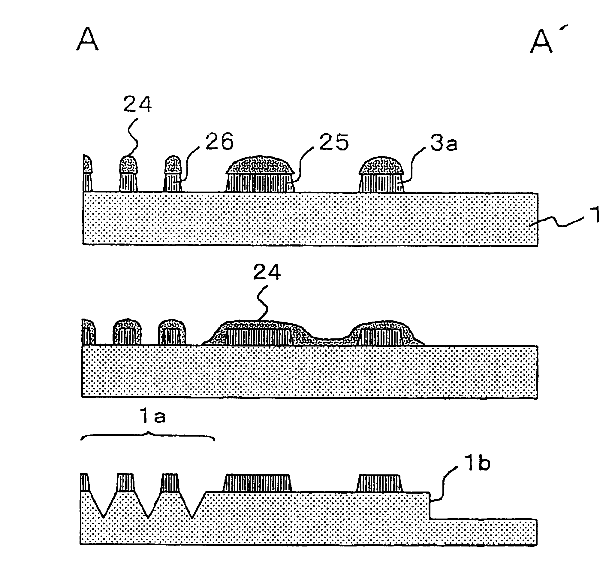
[0180]Referring first to FIGS. 16, 23a, 25a, 27a, 29a and 31a, a gate electrode layer (Cr layer, not shown), which later becomes underlying metal layers 2a, 3a, 17a, 18a, 19a, 20d, 20e, 21a, 25 and 26, is formed on the entire surface of the insulating substrate 1 having a planar surface.

[0181]Referring to FIGS. 16, 23a, 25a, 27a, 29a and 31a, a first mask 24 is formed on the gate electrode layer by a photolithography technique. Then, unneeded portions of the gate electrode layer are removed by for example dry etching or wet etching. This forms the gate bus line 2, gate electrode 3, underlying metal layer 17a of the gate terminal unit, underlying metal layer 18a of the drain terminal unit, underlying metal layer 19a of the common terminal unit, gate electrodes 20d, 20e for the common device unit, common bus line 21 for the drain, shorting prohibiting wiring 25 and...

third embodiment

[0210]The production process for the active matrix substrate in the liquid crystal display apparatus is now explained.

[0211]Referring first to FIGS. 33, 39a, 41a, 43a, 44a and 45a, a gate electrode layer (Cr layer, not shown), which later becomes underlying metal layers 2a, 3a, 17a, 18a, 19a, 20d, 20e and 21a, is formed on the entire surface of the insulating substrate 1 having a planar surface.

[0212]Referring to FIGS. 33, 39a, 41a, 43a, 44a and 45a, a first mask 24 is formed on the gate electrode layer by a photolithography technique. Then, unneeded portions of the gate electrode layer are removed by for example dry etching or wet etching. This forms the gate bus line 2, gate electrode 3, underlying metal layer 17a of the gate terminal unit, underlying metal layer 19a for the common terminal unit, gate electrodes 20d, 20e for the common device unit and the common bus line 21 for the drain. At this stage, the first mask 24 has not been removed.

[0213]Referring to FIGS. 33, 39b, 41b,...


PUM

PropertyMeasurementUnit
surface roughnessaaaaaaaaaa
thicknessaaaaaaaaaa
thicknessaaaaaaaaaa

Abstract

To provide a liquid crystal display apparatus exhibiting optimum display performance despite reduction in the number of PR(photolithography) processes, and a method for producing the apparatus. A method for producing a liquid crystal display apparatus having a first substrate including a thin film transistor and a reflector on an insulating substrate. An etching mask is formed on a metal layer formed on the insulating substrate and, using this etching mask, the metal layer is etched to form a constituent portion of the thin film transistor and protrusions. Only the etching mask is caused to reflow to cover exposed surface portions of the constituent portion of the thin film transistor and protrusions and near-by surface portions of the insulating substrate with the etching mask as the insulating substrate is partially exposed. Using the etching mask, recesses are formed in an exposed area of the insulating substrate. A reflector is formed on the protrusions and recesses.

Description

FIELD OF THE INVENTION[0001]This invention relates to a method for producing a liquid crystal display apparatus having a reflection type panel or a half-transmitting type panel. More particularly, it relates to a method for producing a liquid crystal display apparatus having an optimum display function with simplified processes.BACKGROUND OF THE INVENTION[0002]A liquid crystal display apparatus, employing active devices, such as thin-film transistors, features a thin thickness and a light weight, and is exploited as a high picture quality flat panel display. With the liquid crystal display apparatus, it is being contemplated to simplify the manufacturing process for realization of low production cost.[0003]The liquid crystal display apparatus is being used as a display unit for a mobile terminal. The liquid crystal display apparatus used currently is predominantly a reflection type or semi-transmitting type liquid crystal display apparatus.[0004]Of these, the reflection type liquid ...

Claims


Application Information

Patent Timeline
Patent Type & Authority Patents(United States)
IPC IPC(8): G02F1/1335G02F1/13G02F1/1362G02F1/1368G09F9/00G09F9/30G09F9/35H01L21/28H01L21/336H01L29/786
CPCG02F1/133553G02F1/1362G02F1/133555G02F1/1368G02F1/136227G02F1/13
Inventor YAMAGUCHI, HIROTAKA
Owner NEC LCD TECH CORP
Why Eureka
Try Eureka