Triode structure field emission display device using carbon nanotubes and method of fabricating the same

a carbon nanotube and display device technology, applied in the manufacture of electrode systems, electric discharge tubes/lamps, discharge tubes luminescnet screens, etc., can solve the problem of reducing the amount of electrons emitted, difficult to achieve a high aspect ratio, and large amount of residues, etc. problem, to achieve the effect of suppressing the short circuit between electrodes

Inactive Publication Date: 2005-02-24
SAMSUNG SDI CO LTD
View PDF9 Cites 28 Cited by
  • Summary
  • Abstract
  • Description
  • Claims
  • Application Information

AI Technical Summary

Benefits of technology

[0025] The present invention provides a field emission display device in which a short circuit can be prevented from occurring between a gate electrode and a cathode by removing an alignment error between the gate electrode and the carbon nanotubes which may occur during a high-temperature firing process.
[0026] The present invention also provides a method of fabricating a field emission display device, through which a carbon nanotube residue, which may cause a short circuit between electrode and diode emission, is prevented from being produced during a carbon nanotube paste development process.
[0036] The present invention removes an alignment error between a gate electrode pattern and a cathode pattern, which may occur during a high-temperature firing process in fabricating a field emission display device, thereby preventing short circuit between the gate electrode and the cathode.
[0037] In addition, the present invention provides a method of fabricating a field emission display device, in which a protective layer is formed to protect the surface of the cathode and prevent carbon nanotube paste from being remaining during development of the carbon nanotube paste, thereby suppressing short circuit between electrodes and electron emission of an anode.

Problems solved by technology

Due to an alignment error between the gate electrode 6 and the electron emitting source 31, the gate electrode 6 may become in contact with or very close to the ITO cathode layer 2, resulting in current leak or a decrease in the amount of electrons emitted.
When the method of performing direct alignment and injecting carbon nanotube paste is used, it is difficult to achieve a high aspect ratio due to an alignment error in equipment and viscosity of a carbon nanotube material.
In the rear exposure method, since a sacrificial layer is not used, a large amount of residues are produced.

Method used


Image

  • Triode structure field emission display device using carbon nanotubes and method of fabricating the same
  • Triode structure field emission display device using carbon nanotubes and method of fabricating the same
  • Triode structure field emission display device using carbon nanotubes and method of fabricating the same

Examples


first embodiment

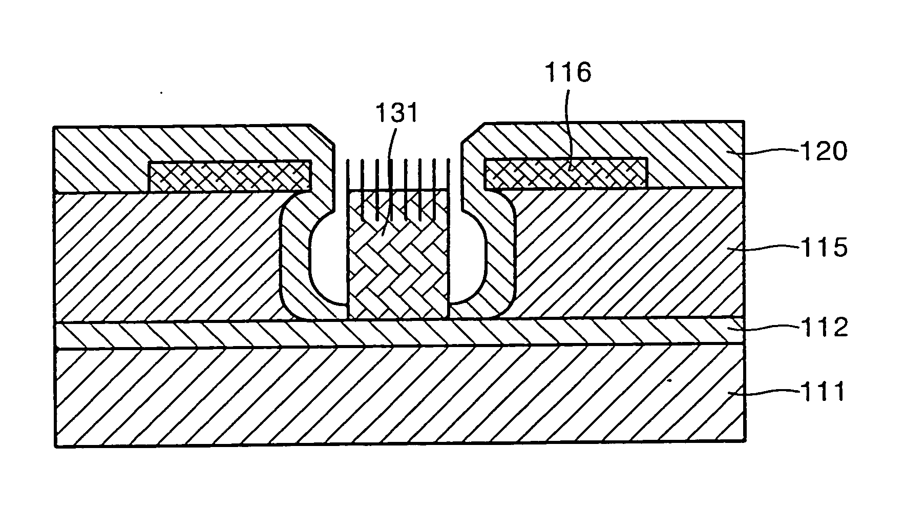
[0050]FIGS. 5A through 5R are diagrams of a method of fabricating the field emission display device shown in FIG. 4 according to the present invention.

[0051] As shown in FIG. 5A, the cathode layer 112 of indium tin oxide (ITO) is deposited on the substrate 111. As described above, the cathode layer 112 is formed of a transparent conductive material for rear exposure.

[0052] Next, as shown in FIG. 5B, the insulation layer 115 is deposited on the cathode layer 112, and firing is performed at high temperature over 550° C. Unlike a conventional method of fabricating a field emission display device, in the first embodiment of the present invention, a mask cathode layer is removed; immediately the insulation layer 115 is deposited on the cathode layer 112; and a firing process is performed before forming a cathode pattern. Accordingly, an alignment error between the cathode pattern and a gate electrode pattern does not occur.

[0053] After the firing process, as shown in FIG. 5C, the gate ...

second embodiment

[0063]FIGS. 7A through 7H are diagrams of a method of fabricating a field emission display device according to the present invention.

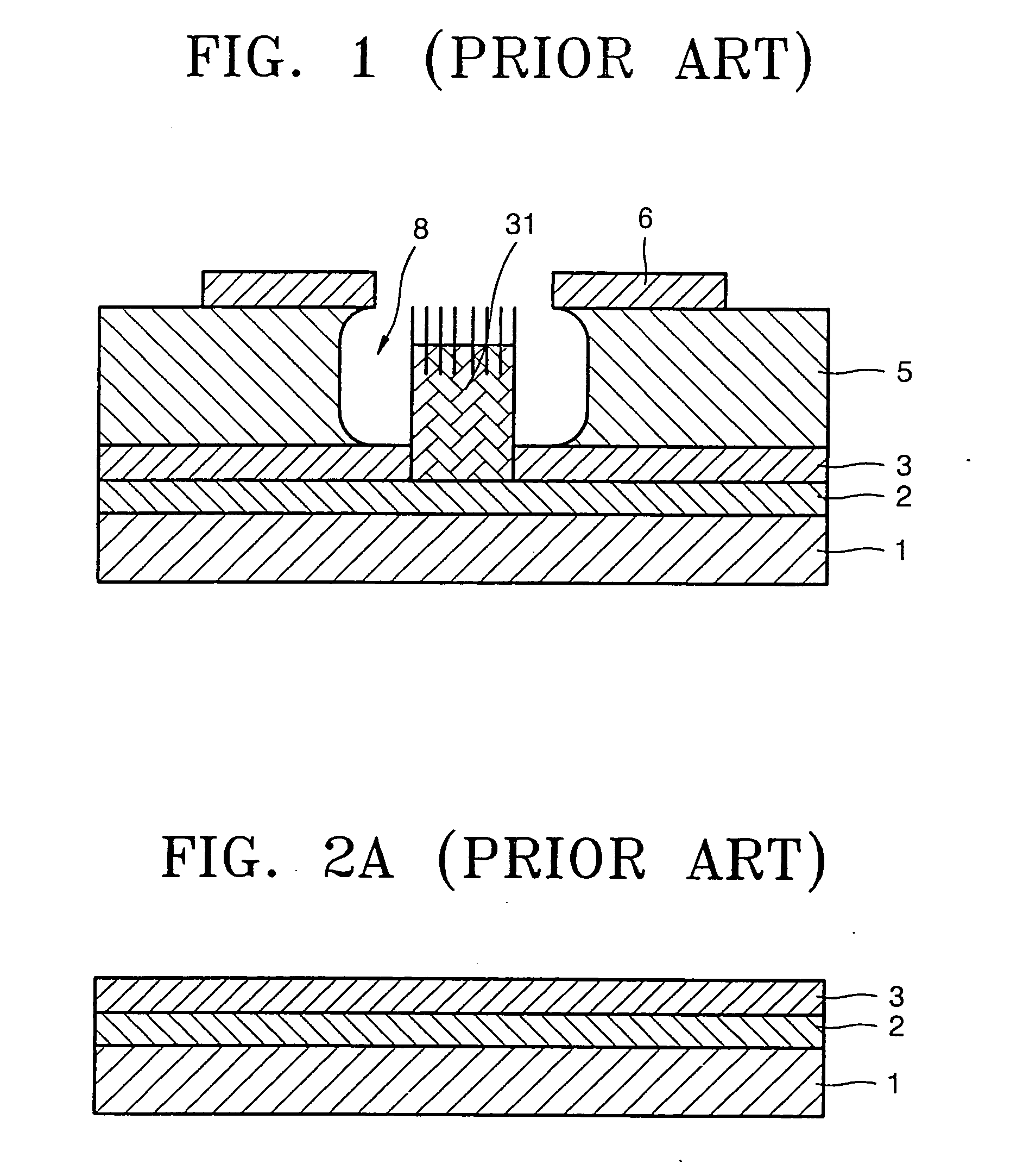
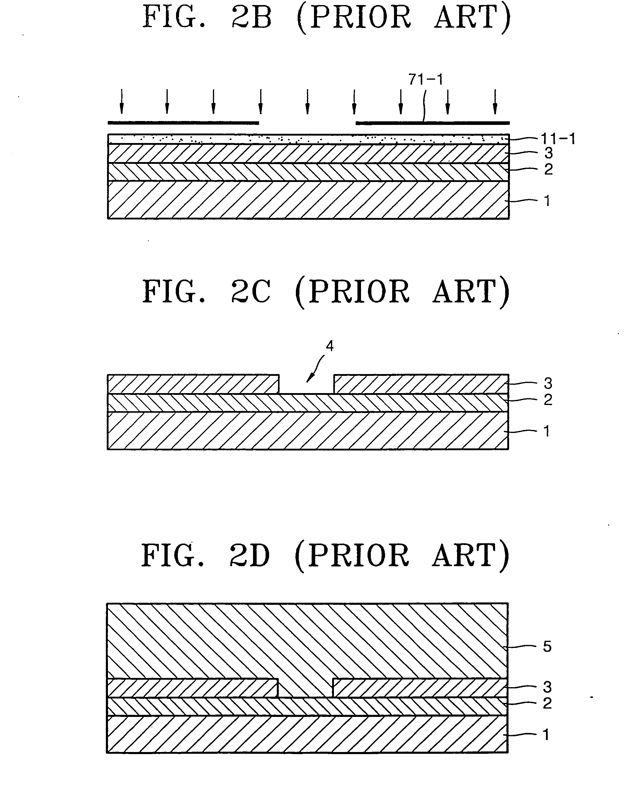
[0064]FIG. 7A shows a triode structure of a conventional field emission display device as shown in FIG. 2J. Reference numeral 211 denotes a substrate. Reference numeral 212 denotes an ITO electrode layer. Reference numeral 213 denotes a mask cathode layer. Reference numeral 215 denotes an insulation layer. Reference numeral 216 denotes a gate electrode. Reference numeral 218 denotes a well.

[0065] As shown in FIG. 7B, a material such as a dry film release (DFR) film which is a kind of photoresist and remains during developer treatment is deposited to cover the insulation layer 215 and the gate electrode 216, thereby forming a protective layer 217, and a mask 271 is disposed on the protective layer 217. Then, the protective layer 217 is patterned by a photoprocess including exposure and development, thereby forming a well 218′, as shown in FIG. 7C.

[006...


PUM

PropertyMeasurementUnit
temperatureaaaaaaaaaa
transparentaaaaaaaaaa

Abstract

A field emission display device and a method of fabricating the same are provided. The field emission display device includes a substrate, a transparent cathode layer, an insulation layer, a gate electrode, a resistance layer, and carbon nanotubes. The transparent cathode layer is deposited on the substrate. The insulation layer is formed on the cathode layer and has a well exposing the cathode layer. The gate electrode is formed on the insulation layer and has an opening corresponding to the well. The resistance layer is formed to surround the surface of the gate electrode and the inner walls of the opening and the well so as to block ultraviolet rays. The carbon nanotube field emitting source is positioned on the exposed cathode layer. An alignment error between the gate electrode and the cathode is removed, and carbon nanotube paste is prevented from remaining during development, thereby preventing current leakage and short circuit between the electrodes and diode emission. Accordingly, the performance of the field emission display device can be improved.

Description

CROSS-REFERENCE TO RELATED APPLICATIONS [0001] This application claims the priority of Korean Patent Application No. 2002-3687, filed on Jan. 22, 2002, which is incorporated herein in its entirety by reference. BACKGROUND OF THE INVENTION [0002] 1. Field of the Invention [0003] The present invention relates to a field emission display device having carbon nanotubes and a method of fabricating the same, and more particularly, to a field emission display device in which an alignment error between a gate electrode and a cathode electrode due to high-temperature firing does not occur, and a method of fabricating the same. [0004] 2. Description of the Related Art [0005] Display apparatuses used for personal computers (PCs) and television receivers include cathode-ray tubes, liquid crystal displays (LCDs), plasma display panels (PDPs), and field emission displays (FEDs), which use high-speed thermionic emission. [0006] FEDs using carbon nanotubes is much more advantageous than cathode-ray...

Claims


Application Information

Patent Timeline
Patent Type & Authority Applications(United States)
IPC IPC(8): H01J1/30H01J1/304H01J9/02
CPCB82Y10/00H01J1/304Y10S977/952H01J2201/30403H01J9/025C01B32/05H01J1/30B82Y40/00
Inventor LEE, HANG-WOOLEE, SANG-JINPARK, SHANG-HYEUN
Owner SAMSUNG SDI CO LTD
Why Eureka
Try Eureka