Solar cell and method for manufacturing same

a solar cell and solar cell technology, applied in the field of solar cells, can solve the problems of difficult to insulate the emitter doping in the region of the provided back-side emitter busbar with respect to the adjacent back-side doping (bsf), and achieve the effect of reliable manufacturing and high yield

Inactive Publication Date: 2011-10-20
ROBERT BOSCH GMBH
View PDF2 Cites 23 Cited by
  • Summary
  • Abstract
  • Description
  • Claims
  • Application Information

AI Technical Summary

Benefits of technology

[0010]An object of the present invention is to provide an improved solar cell which is contacted completely from the back side, and which may be reliably manu

Problems solved by technology

In addition, this makes it difficult to also insulate the emitter doping in a strip in the regio

Method used


Image

  • Solar cell and method for manufacturing same
  • Solar cell and method for manufacturing same
  • Solar cell and method for manufacturing same

Examples


Embodiment Construction

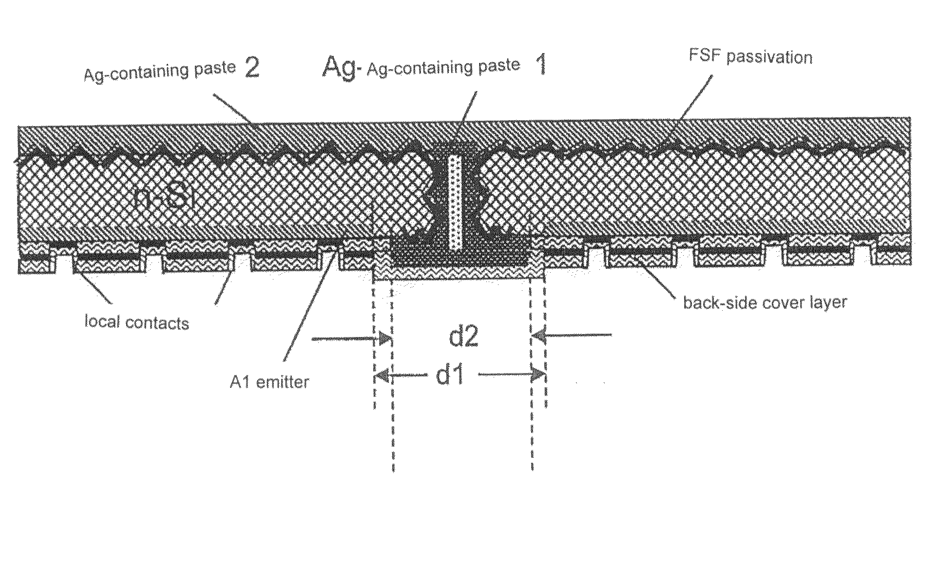
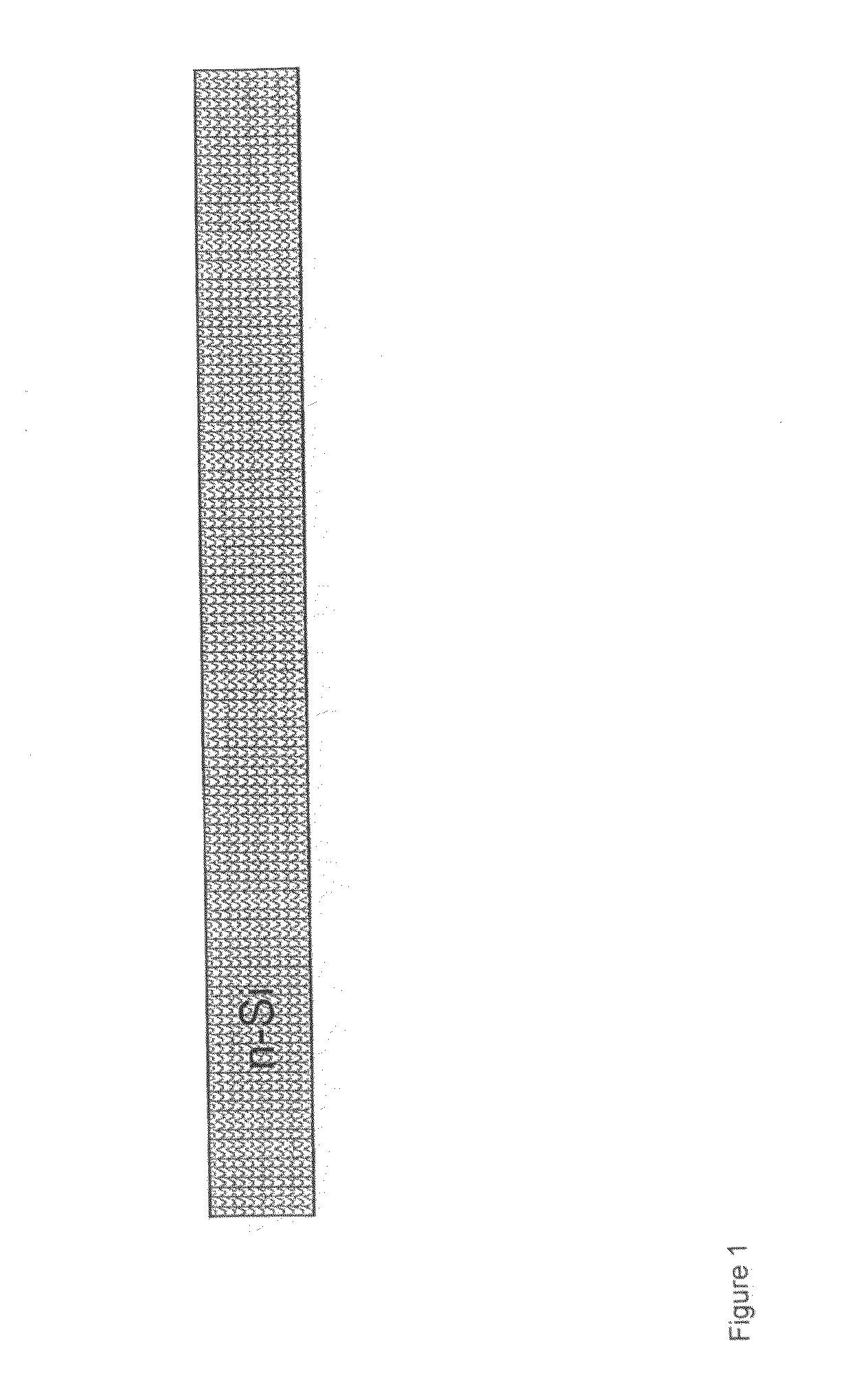
[0026]FIGS. 1 through 21 show schematic detail illustrations of one example embodiment of the solar cell and the manufacturing method according to the present invention, in cross sections or bottom views (top views of the second main surface). Due to the illustrated coating sequence, the individual figures for the most part are self-explanatory; therefore, the following description is provided merely in outline form and is understood to be a supplement to the figures.

[0027]In particular, the measures known from the related art for providing selective doping beneath the silver fingers on the front side have not been included in the description, without ruling out that these measures may be used in the cell according to the present invention in order to improve the blue light sensitivity on the front side.

[0028]Starting with a roughly purified n-silicon wafer, the following process steps (as an example) result in one preferred specific embodiment of the described cell concept.

[0029]1)...


PUM


Abstract

A solar cell an n-doped silicon substrate, having n+ base regions provided in the first main surface and a p+ doped emitter region provided in the second main surface, a finger-like base contact structure applied to the first main surface, an emitter contact and base contact paths applied to the second main surface, each having solderable contact surfaces as well as through-connections (vias) which connect the finger-like contact structure of the first main surface to the base contact paths on the second main surface, thus connecting the emitter region as well as the base regions via the solder contact surfaces on the second main surface. The second main surface is free from p+ emitter doping in places, and the first main surface and predetermined regions of the second main surface have an n+n transition.

Description

BACKGROUND OF THE INVENTION[0001]1. Field of the Invention[0002]The present invention relates to a solar cell having an n-doped semiconductor substrate, in particular made of silicon, having base regions on the front side, a finger-like base contact structure applied to the front side, base contact paths on the back side, and through-connections (vias) which connect the finger-like contact structure to the contact paths, and a method for manufacturing same.[0003]2. Description of Related Art[0004]Solar cells having contact fingers on the front side which are connected via laser-bored, metal-filled holes to solderable contact paths (busbars) on the back side have been known for quite some time (Patent Abstracts of Japan, Publication No. 58-039071 (1983); Patent Abstracts of Japan, Publication No. 04223378 (1992)). These solar cells, referred to as metal wrap through (MWT) cells, are provided on p-doped base material which is usually multicrystalline, and which has an emitter that is ...

Claims


Application Information

Patent Timeline
IPC IPC(8): H01L31/0224H01L31/18H01L31/068
CPCH01L31/02167H01L31/022425Y02E10/547H01L31/0236H01L31/068H01L31/02245H01L31/02363
Inventor KROKOSZINSKI, HANS-JOACHIM
Owner ROBERT BOSCH GMBH
Why Eureka
Try Eureka