

Dynamic Focus Adjustment with Optical Height Detection Apparatus in Electron Beam system
a technology of height detection and dynamic focus, applied can solve the problems of too slow time of adjusting the focus by varying the lens current, image blurring, and the disadvantage of capacitance gage in the field of electron beam system
- Summary
- Abstract
- Description
- Claims
- Application Information
AI Technical Summary
Benefits of technology
Problems solved by technology
Method used
Image

Examples
Embodiment Construction
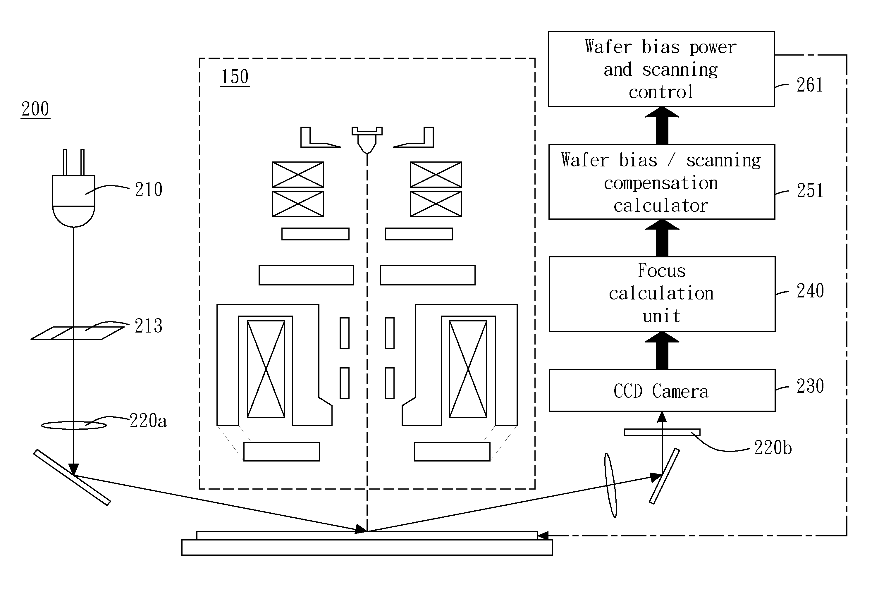
[0022]The present invention generally relates to dynamic focus adjustment for an image system. With the assistance of a height detection system, present invention provides an apparatus and methods for micro-adjusting an image focus according the specimen surface height variation by altering the field strength of an electrostatic lens between objective lens and sample stage or by altering a bias voltage applied to the sample surface. Merely by way of example, the invention has been applied to a scanning electron inspection system. But it would be recognized that the invention could apply to other systems using charged particle beam as observation tool with a height detection apparatus.
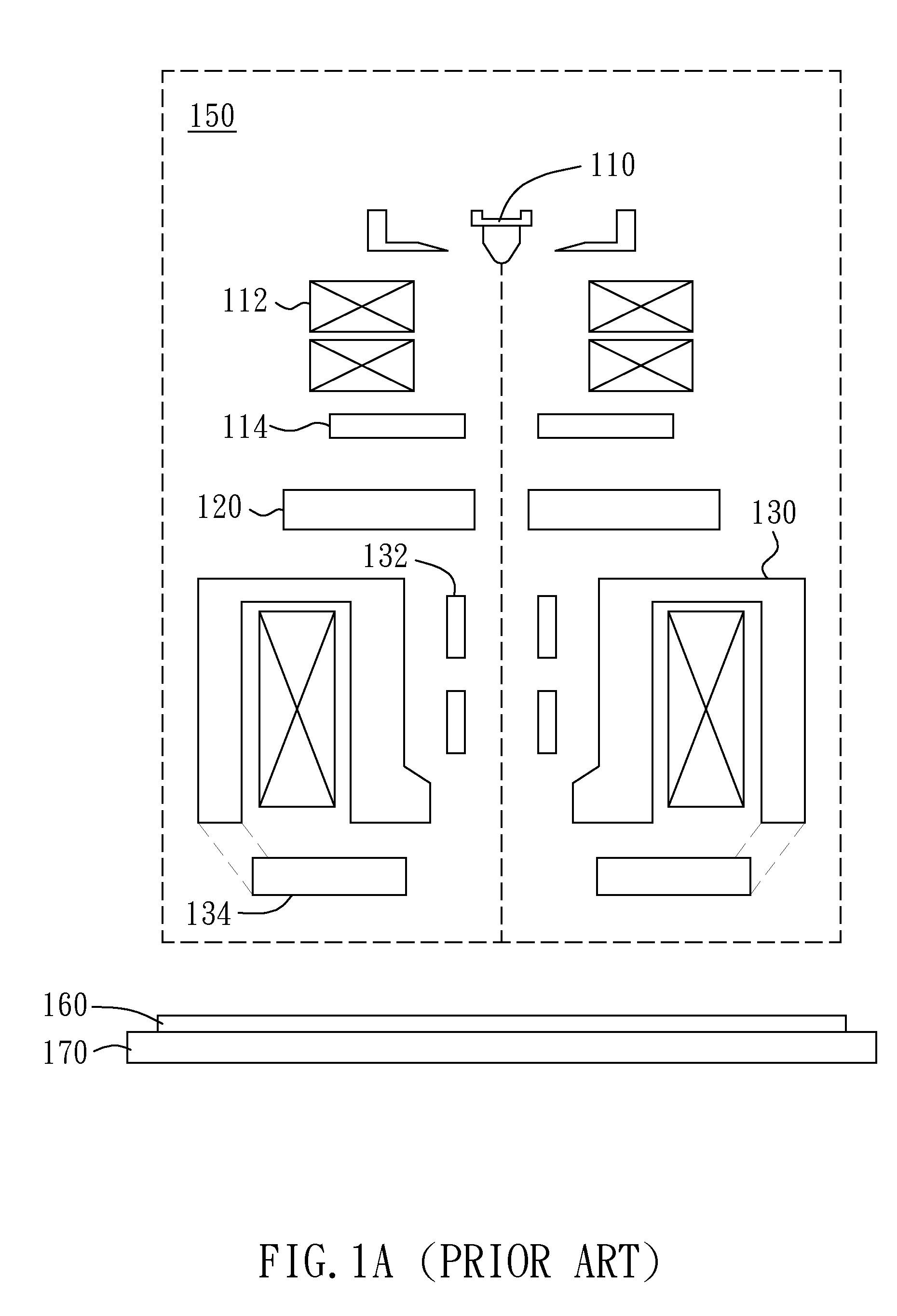
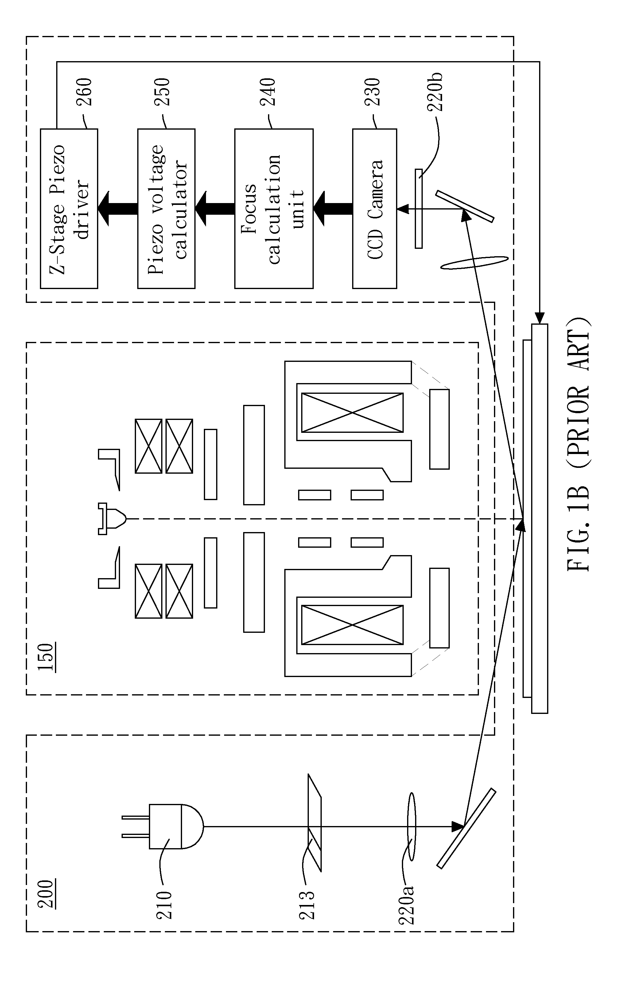
[0023]The system configuration of the present invention is illustrated in FIG. 1A and FIG. 1B which includes a regular e-beam inspection system 150 to perform inspection and a height detection sub-system 200 to assist focusing. Detail of the e-beam system 150 comprises electron source 110, condenser len...
PUM
 Abstract
Description
Claims
Application Information