

Semiconductor device and bypass capacitor module
a technology of capacitor module and semiconductor device, which is applied in the direction of basic electric elements, transistors, and fixed capacitor combinations of structural structures, can solve the problems of increasing the cost and size of capacitors, and the operating limit at a high frequency
- Summary
- Abstract
- Description
- Claims
- Application Information
AI Technical Summary
Benefits of technology
Problems solved by technology
Method used
Image

Examples
first embodiment
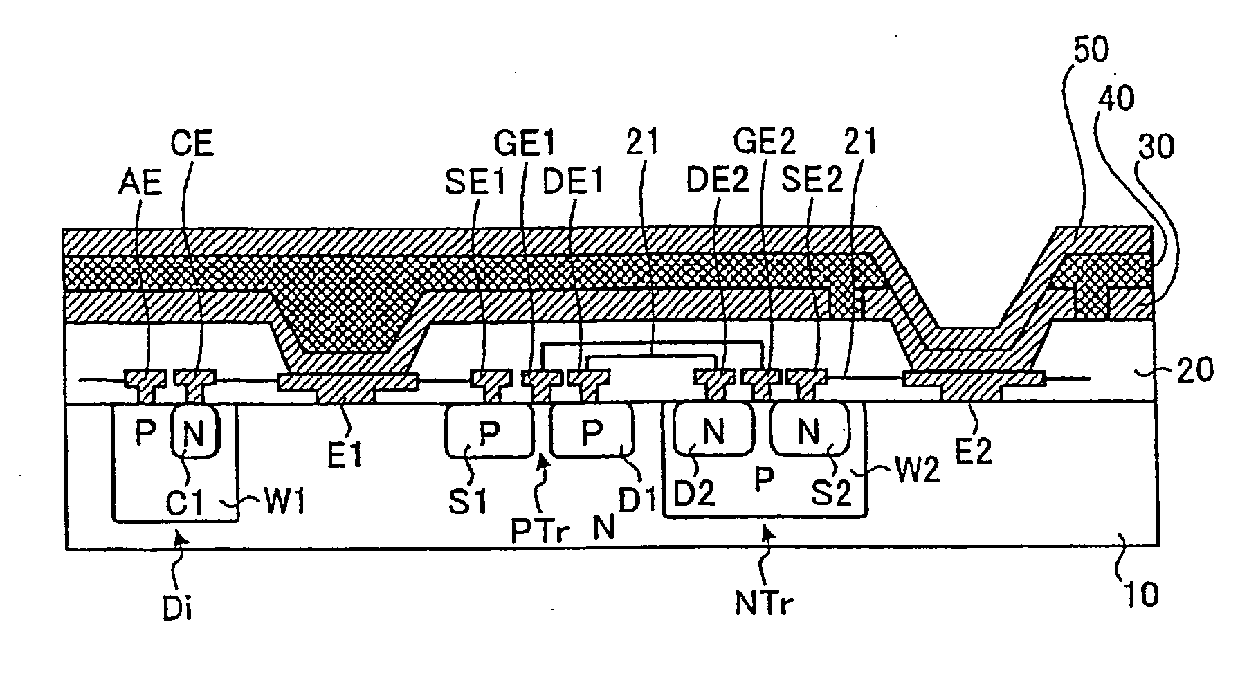
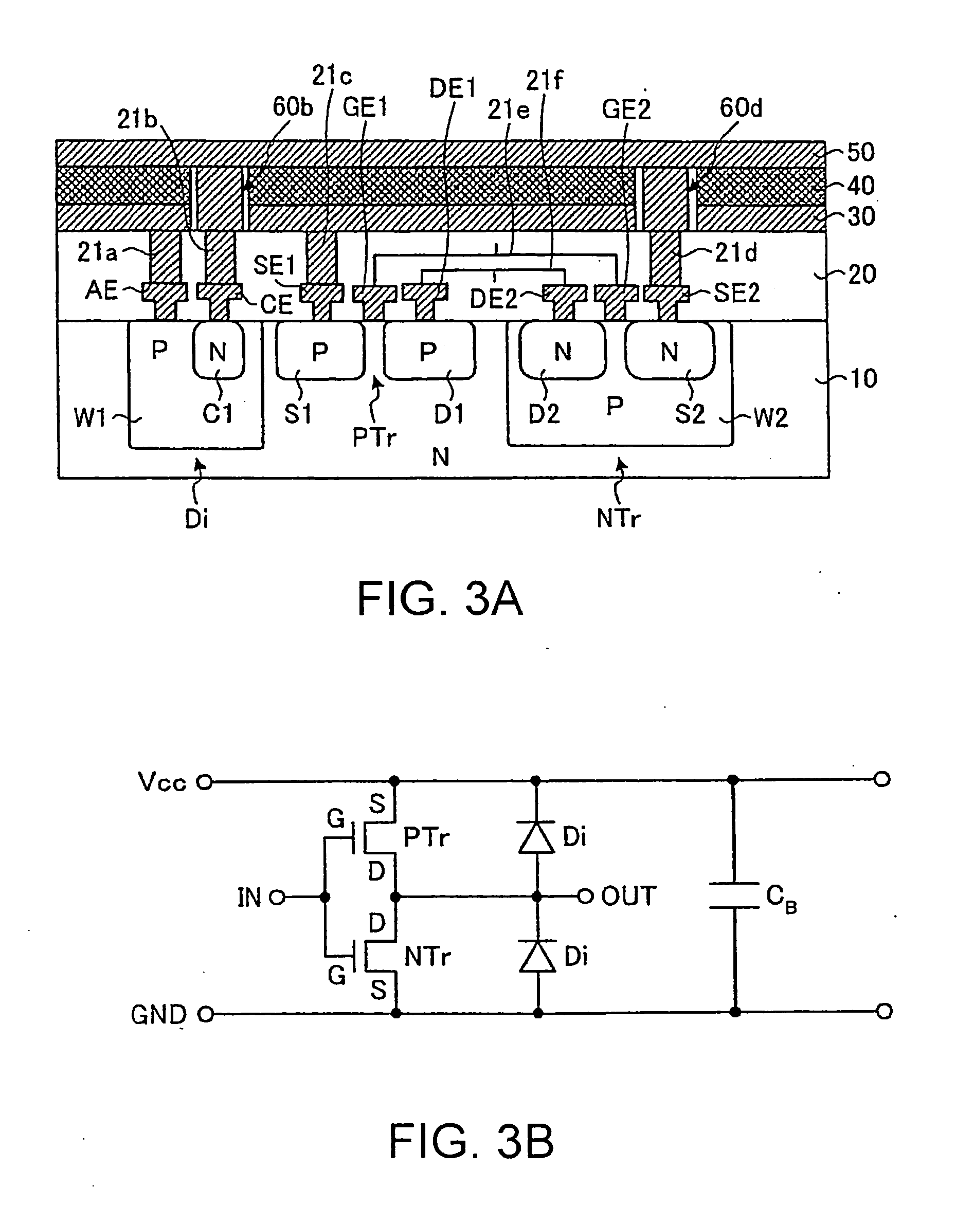
[0039]Referring to FIGS. 3A to 5F, a semiconductor device according to a first embodiment will be described. In the semiconductor device according to the first embodiment, a CMOS transistor and a diode are mounted on a substrate as semiconductor elements.
[0040]Referring to FIG. 3A, a Si substrate 10 is doped with an -type dopant of a low concentration. The Si substrate 10 is provided with a CMOS transistor and a diode Di. The CMOS transistor comprises a P-channel MOS transistor PTr and an -channel MOS transistor NTr in an integrated structure.
[0041]The P-channel MOS transistor PTr comprises a source region S1 and a drain region D1 which are formed by diffusing a P-type dopant of a high concentration, a source electrode SE1, a drain electrode DE1, and a gate electrode GE1. Although not shown in all of figures for simplicity of illustration, it is to be noted that a gate insulating film underlies each gate electrode, such as GE1.
[0042]The N-channel MOS transistor NTr comprises a P-typ...
second embodiment
[0059]Referring to FIGS. 6 to 7E, a semiconductor device according to a second embodiment of this invention will be described. In the semiconductor device according to the first embodiment, the Vcc power supply layer 30 is formed throughout an entire surface of the Si substrate 10. On the other hand, in the semiconductor device according to the second embodiment, a Vcc power supply layer 30 is separated into sections corresponding to a plurality of predetermined circuit blocks. Similar parts equivalent in functions to those in FIG. 3A are designated by like reference numerals and description thereof will be omitted.
[0060]Referring to FIG. 6, an insulating layer 20 is provided with an electrode E1 connected to the Vcc power supply layer 30 and an electrode E2 connected to the GND layer 50. The electrode E1 is connected via a wire 21 to a source electrode SE1 of a P-channel MOS transistor PTr and a cathode electrode CE of a diode Di. The electrode E2 is connected via the wire 21 to a ...
third embodiment
[0066]Referring to FIG. 8, a semiconductor device according to a third embodiment of this invention will be described. In the semiconductor device according to the first embodiment, the bypass capacitor is formed on one surface of the Si substrate 10 on which the semiconductor elements are formed. On the other hand, in the semiconductor device according to the third embodiment, a bypass capacitor is formed on the other surface of the Si substrate 10 opposite to the one surface on which the semiconductor elements are formed. The one surface provided with the semiconductor elements and the other surface without the semiconductor elements may be referred to as a first surface and a second surface, respectively.
[0067]In FIG. 8, similar parts equivalent in function to those in FIG. 3A are designated by like reference numerals and description thereof will be omitted. In the figure, the Si substrate 10 has a first surface provided with semiconductor elements and a second surface opposite t...
PUM
 Abstract
Description
Claims
Application Information