Charge storage device architecture for increasing energy and power density

a technology of energy storage and power density, applied in the direction of fuel and primary cells, cell components, transportation and packaging, etc., can solve the problems of inability to show exciting improvement in energy or power performance, limited energy density by its effective double-layer area, and high scanning rate capacitan

Inactive Publication Date: 2011-10-27
RGT UNIV OF CALIFORNIA
View PDF21 Cites 39 Cited by
  • Summary
  • Abstract
  • Description
  • Claims
  • Application Information

AI Technical Summary

Benefits of technology

[0019]In certain embodiments of the present invention, it may be advantageous to have a multilayered electrode structure, in which a portion of a

Problems solved by technology

For a DLS, the rapid charge/discharge process provides the capacitor with a high power density, yet the energy density is limited by its effective double-layer area.
However, the capacitance may drop dramatically at high scanning rates because of their tortuous pore structure and high microporosity.
The templated carbons, on the other hand, exhibit uniform pore geometry and larger pore size; however, they did not show any exciting improvement in either energy or power performance.
However, actual applications of ECS are still limited by high cost, low operation voltage, or poor rate capability, mostly because of inefficient mass transport

Method used


Image

  • Charge storage device architecture for increasing energy and power density
  • Charge storage device architecture for increasing energy and power density
  • Charge storage device architecture for increasing energy and power density

Examples


example 1

A Carbon Nanotube Film as DLS Material

[0081]In certain embodiments of the present invention, a charge storage device may comprise a CNT film as a DLS material.

[0082]SWNTs were dissolved in pure water (1-2 mg / ml) with the aid of a tip sonicator. Using an air brush pistol the stable suspension was sprayed onto overhead transparencies (polyethylene-terephthalate, PET) which were placed on a heating plate at ˜100° C. During spraying, the water evaporates and the CNTs form an entangled random network on the PET. Afterwards the CNT coated PET substrates were used as the carbonaceous nanostructured network (DLS material) without any further treatment.

[0083]A polymer electrolyte was prepared by mixing polyvinyl alcohol (PVA) with water (1 g PVA / 10 ml H2O) and subsequent heating under stirring to ˜90° C. until the solution becomes clear. After cooling down, conc. phosphoric acid was added (0.8 g) and the viscose solution was stirred thoroughly. Finally, the clear solution can be cast into a ...

example 2

Carbonaceous Networks Together with ECS Materials

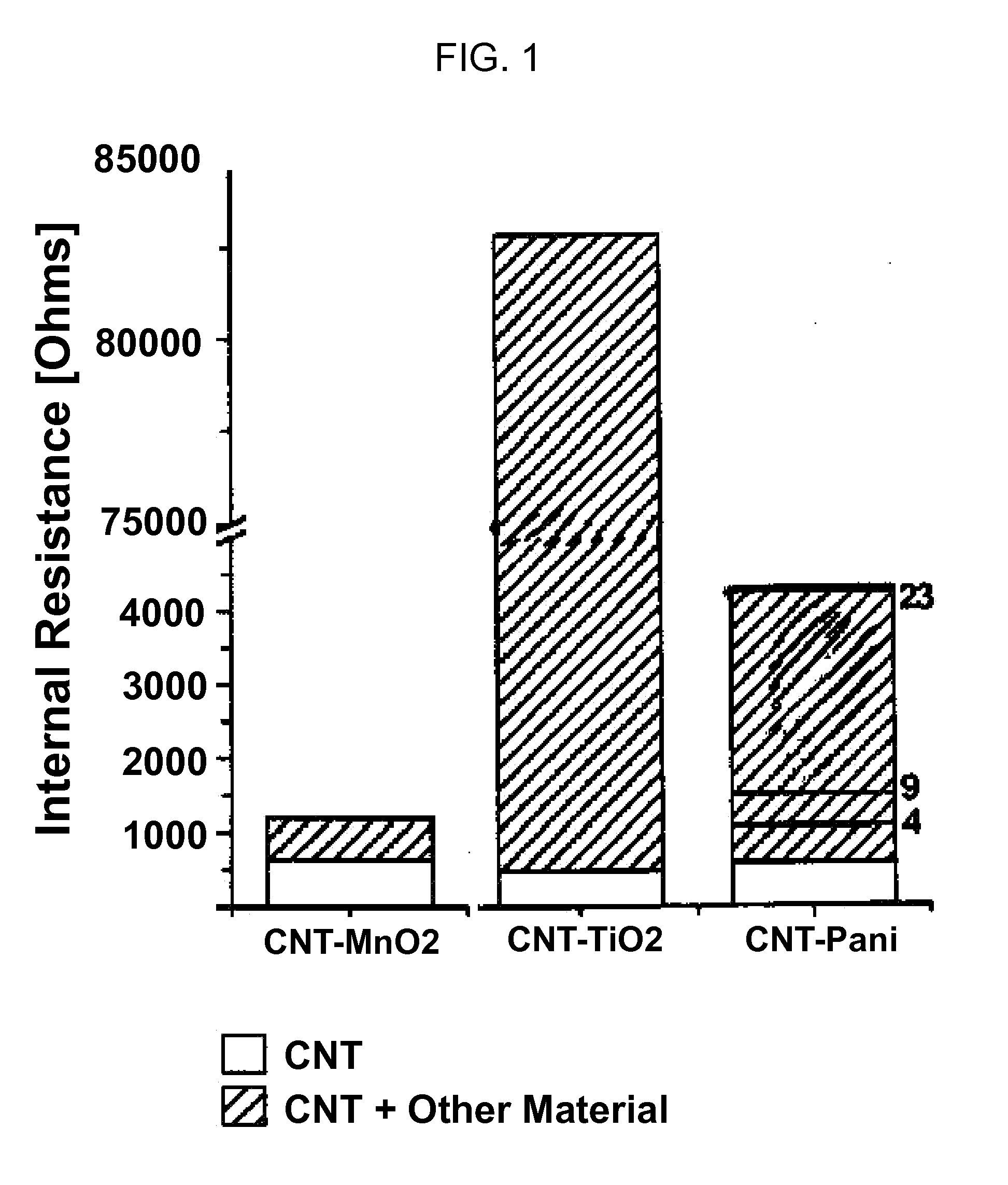
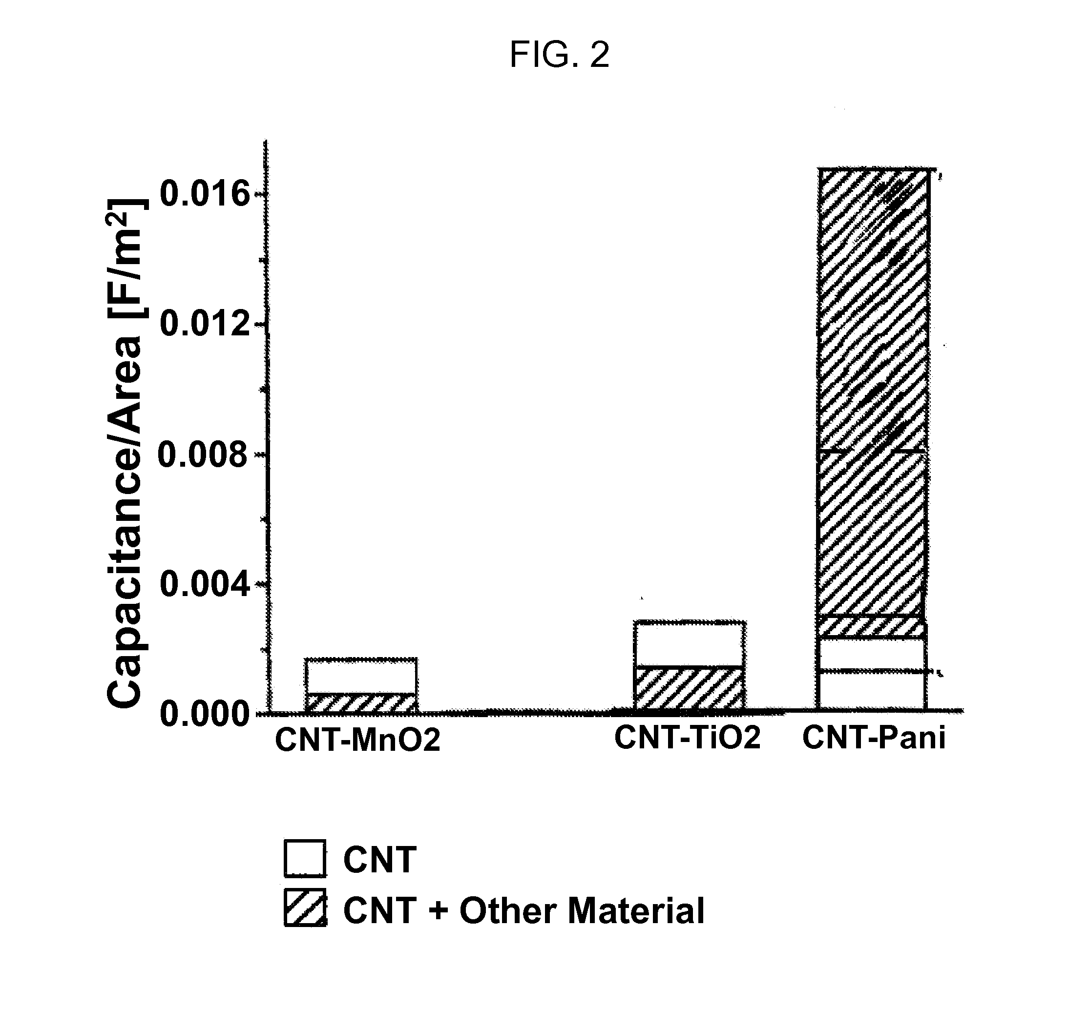
[0084]Use of a DLS material in combination with an ECS material in a charge storage device electrode may take advantage of both the high conductivity of the CNT networks and the high specific capacitance of the coating potentially increasing the capacitance of CNT networks. The ECS material was sprayed on top of the CNT networks. In such a multiple network the CNT network can act not only as a DLS material, but also as a current collector (e.g., where the additional ECS material coating is the active material). This multilayer structure is fundamentally different from composites where all materials (e.g., DLS material and ECS material) are mixed together, potentially interrupting the current conducting paths within the CNT network. The performance of these multiple networks is evidenced in FIGS. 1 and 2 in terms of internal resistance and capacitance / area, respectively.

[0085]When using inorganic coatings as an ECS material, here MnO2 ...

example 3

Electrode Device with CNT and Carbon / Polyaniline (PANI) Electrodes

[0087]In an experimental embodiment of the present invention, a three-layer structure, with CNTs as one electrode and a two-layer CNT / polyaniline (PANI) structure as a second electrode, was fabricated and compared with a symmetric DLS architecture with two electrodes formed from CNTs.

[0088]A SWNT suspension (1.0 mg CNTs / ml in deionized water) was sprayed onto polyethyleneterephthalate (PET) which was heated at temperature about 120° C. The spayed film was ready to use as a working electrode in the PANI electrodeposition; its resistance was around 1000 as measured by a two-probe multi-meter. The thickness of the SWNT film was roughly 1 μm. The electrodeposition of PANI was carried out using a three-electrode electrochemical cell with an Ag / AgCl reference electrode and a platinum sheet as the auxiliary electrode. The PANI film was electrodeposited using cyclic sweep with a GillAC device (AutoAC, ACM Instruments, UK) in ...


PUM


Abstract

Provided is a new charge storage device structure, incorporating a double layer supercapacitor (DLS) material, electrochemical supercapacitor (ECS) material and/or battery material. More specifically, the DLS material, ECS material and/or battery material may form multilayer electrode structures. Additionally or alternatively, the DLS material, ECS material and/or battery material may form electrode structures in which the DLS material, ECS material and/or battery material are in contact with both a common current collector and electrolyte. The present invention can be generalized towards other energy storage devices, opening a new avenue for a large spectrum of device applications.

Description

CROSS-REFERENCE TO RELATED APPLICATIONS[0001]This application a 35 U.S.C. §111(a) continuation of PCT international application serial number PCT / US2009 / 055910 filed on Sep. 3, 2009, incorporated herein by reference in its entirety, which is a nonprovisional of U.S. provisional patent application Ser. No. 61 / 094,353 filed on Sep. 4, 2008, incorporated herein by reference in its entirety. Priority is claimed to each of the foregoing applications.[0002]The above-referenced PCT international application was published as PCT International Publication No. WO 2010 / 028162 published on Mar. 11, 2010 and republished on May 25, 2010, and is incorporated herein by reference in its entirety.STATEMENT REGARDING FEDERALLY SPONSORED RESEARCH OR DEVELOPMENT[0003]Not ApplicableINCORPORATION-BY-REFERENCE OF MATERIAL SUBMITTED ON A COMPACT DISC[0004]Not ApplicableNOTICE OF MATERIAL SUBJECT TO COPYRIGHT PROTECTION[0005]A portion of the material in this patent document may subject to copyright protectio...

Claims


Application Information

Patent Timeline
IPC IPC(8): H01G9/155B82Y99/00
CPCH01G11/02Y02T10/7022H01G11/26H01G11/30H01G11/36H01G11/46H01G11/50H01M4/02H01M4/06H01M4/366H01M4/625H01M6/06H01M12/06Y02E60/13H01G11/04Y02E60/10Y02T10/70
Inventor GRUNER, GEORGE
Owner RGT UNIV OF CALIFORNIA
Why Eureka
Try Eureka