Electric transport component, method of manufacturing the same, as well as electro-optical device and opto-electrical device

a technology of transport components and components, applied in the direction of thermoelectric devices, electrical apparatus construction details, electrical apparatus casings/cabinets/drawers, etc., can solve the problems of relatively large metal features on top of the substrate, and achieve the effect of reducing efficiency, reducing the cost of the device efficiency, and reducing the resistance of at least one electrically conductive structur

Inactive Publication Date: 2011-11-10
OLEDWORKS GMBH +1
View PDF9 Cites 9 Cited by
  • Summary
  • Abstract
  • Description
  • Claims
  • Application Information

AI Technical Summary

Benefits of technology

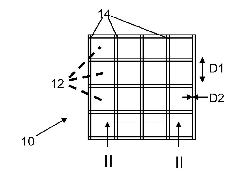
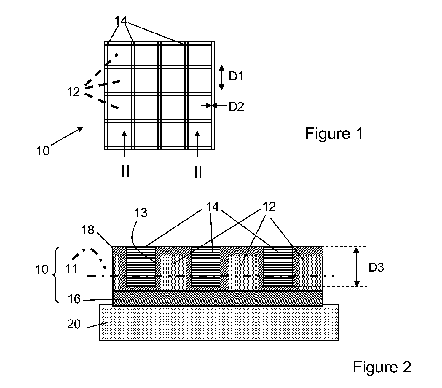
[0013]Where it is desired that the electric transport component is also transmissive, the at least one electrically conductive structure occupies a fraction of the area of the plane of the organic decoupling layer in a range of 0.1 to 20%, said occupied fraction being regularly distributed over the area of the plane. For a substantially larger occupied fraction, e.g. a fraction of 30% the amount of absorbed radiation is relatively high, which would be at the cost of the efficiency of the device, e.g. a photo-voltaic cell or a light-emitting diode, wherein the electric transport component is applied. For a substantially smaller fraction, e.g. a fraction of less than 0.05%, the resistance of the at least one electrically conductive structure would be relatively high, which would also result in a lower efficiency and in the case of a light-emitting device, into an inhomogeneous light-output.
[0014]In an embodiment the at least one electrically conductive structure comprises line shaped segments. Line shaped segments are considered to be curved or straight segments that have a length that is substantially greater, e.g. at least 10 times greater, than their width. In this way a high transmissivity can easily be obtained.

Problems solved by technology

However, these techniques provide metallic features that are on top of the substrate and are relatively large.

Method used


Image

  • Electric transport component, method of manufacturing the same, as well as electro-optical device and opto-electrical device
  • Electric transport component, method of manufacturing the same, as well as electro-optical device and opto-electrical device
  • Electric transport component, method of manufacturing the same, as well as electro-optical device and opto-electrical device

Examples


Embodiment Construction

[0040]In the following detailed description numerous specific details are set forth in order to provide a thorough understanding of the present invention. However, it will be understood by one skilled in the art that the present invention may be practiced without these specific details. In other instances, well known methods, procedures, and components have not been described in detail so as not to obscure aspects of the present invention.

[0041]The terminology used herein is for the purpose of describing particular embodiments only and is not intended to be limiting of the invention. As used herein, the singular forms “a”, “an” and “the” are intended to include the plural forms as well, unless the context clearly indicates otherwise. It will be further understood that the terms “comprises” and / or “comprising,” when used in this specification, specify the presence of stated features, integers, steps, operations, elements, and / or components, but do not preclude the presence or additio...


PUM


Abstract

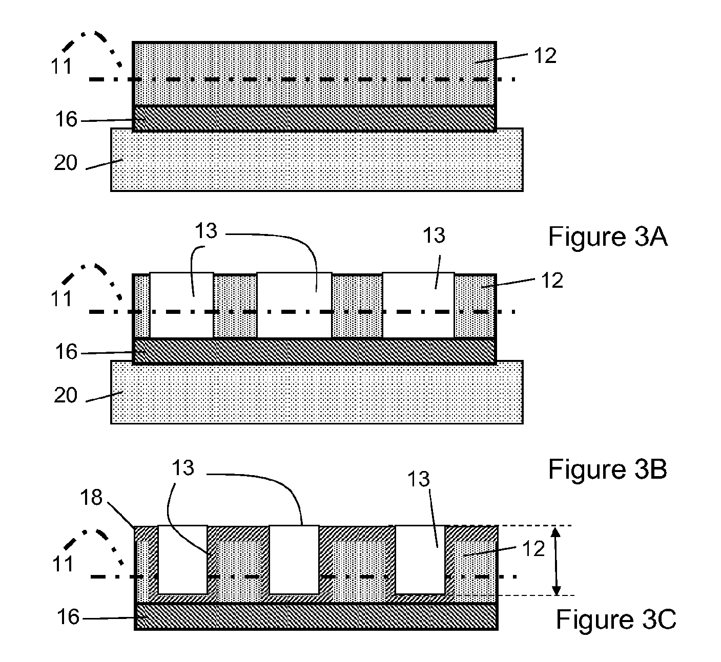
An electric transport component (10; 110; 310; 60) comprises a substrate (20; 120) provided with a barrier structure with a first inorganic layer (16; 116; 66), an organic decoupling layer (12; 112; 62) and a second inorganic layer (18; 118; 68), wherein the organic decoupling layer is sandwiched between the first and the second inorganic layer, and at least one electrically conductive structure (14; 114; 314; 414; 414-1, 414-2; 514; 614-1, 614-2; 64) distributed in a plane defined by the organic decoupling layer, and that is accommodated in at least one trench (13; 113) in the organic decoupling layer.
A method of manufacturing an electric transport component comprises the steps of
  • a) providing a first inorganic layer
  • b) providing a first organic decoupling layer,
  • c) forming at least one trench in the organic decoupling layer,
  • d) depositing an electrically conductive material in the at least one trench,
  • e) providing a second inorganic layer.
The component may be applied for example in opto-electrical and electro-optical devices.

Description

BACKGROUND OF THE INVENTION[0001]1. Field of the Invention[0002]The present invention relates to an electric transport component. The present invention further relates to an electronic device comprising the product. The present invention further relates to a method of manufacturing the product.[0003]2. Related Art[0004]For large area OLED lighting on flexible plastic substrates, a large current is required to drive the system. The present thin film materials used for the anode (e.g. ITO) and cathode (e.g. Ba / Al) have a large resistivity and the large currents give rise to substantial voltage drop, which determine inhomogeneous light emission. For producing large area flexible OLED devices on plastic substrates there is a need for additional metallization structure of the plastic substrate. For reducing the manufacturing costs, such structured metallization coatings will preferably be applied on rolls of plastic foil using an inline roll-to-roll web coating process. Accordingly, for ...

Claims


Application Information

Patent Timeline
Patent Type & Authority Applications(United States)
IPC IPC(8): H05K7/00H01L51/56H01L51/52
CPCH01L51/5203H01L2251/5361H01L2251/5338H10K50/805H10K2102/311
Inventor TANASE, CRISTINADEKEMPENEER, ERIKLIFKA, HERBERTDE VRIES, IKEVAN MOL, ANTONIUS MARIA BERNARDUS
Owner OLEDWORKS GMBH
Why Eureka
Try Eureka