

Simultaneous Multi-Layer Fill Generation
a fill generation and simultaneous technology, applied in the direction of photomechanical treatment originals, instruments, total factory control, etc., can solve the problems of loss of contact, uneven next layer, and variety of circuit structure flaws
- Summary
- Abstract
- Description
- Claims
- Application Information
AI Technical Summary
Benefits of technology
Problems solved by technology
Method used
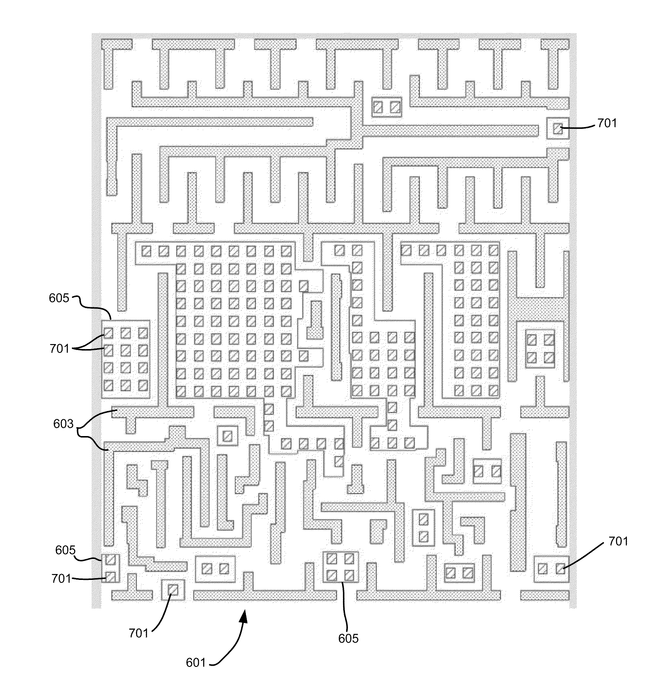
Image

Examples
Embodiment Construction
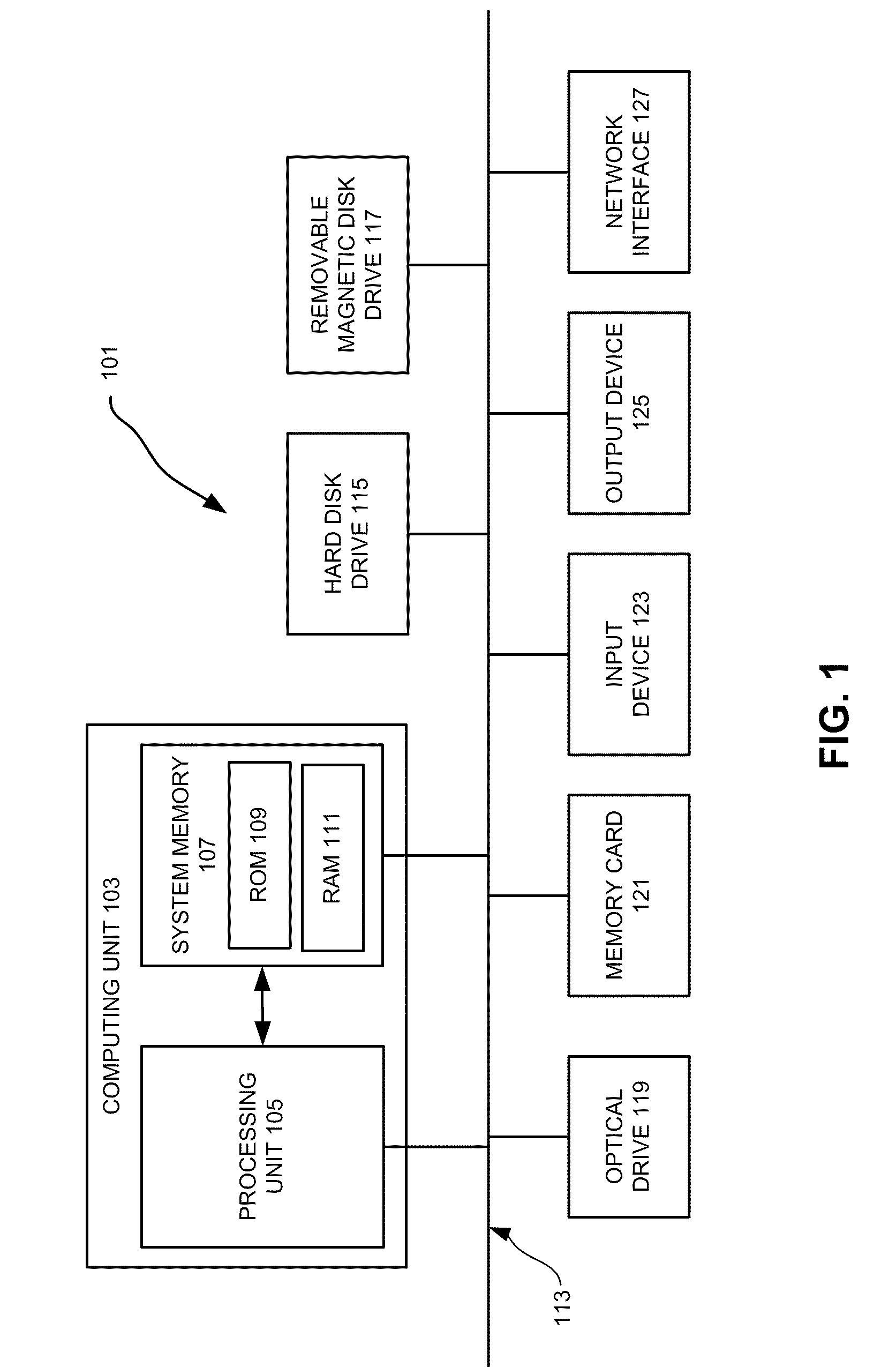
[0027]Various examples of the invention may be implemented through the execution of software instructions by a computing device, such as a programmable computer. Accordingly, FIG. 1 shows an illustrative example of a computing device 101. As seen in this figure, the computing device 101 includes a computing unit 103 with a processing unit 105 and a system memory 107. The processing unit 105 may be any type of programmable electronic device for executing software instructions, but will conventionally be a microprocessor. The system memory 107 may include both a read-only memory (ROM) 109 and a random access memory (RAM) 111. As will be appreciated by those of ordinary skill in the art, both the read-only memory (ROM) 109 and the random access memory (RAM) 111 may store software instructions for execution by the processing unit 105.
[0028]The processing unit 105 and the system memory 107 are connected, either directly or indirectly, through a bus 113 or alternate c...
PUM
 Abstract
Description
Claims
Application Information