Solar cell and solar cell manufacturing method

a solar cell and manufacturing method technology, applied in the field of solar cells, can solve the problems of inability to efficiently extract electrons resulting from photoelectric conversion by quantum dots, loss due to distribution bias, and uneven electric charge distribution, so as to reduce manufacturing costs, reduce carrier loss, and high energy conversion efficiency

Inactive Publication Date: 2011-12-01
FUJIFILM CORP
View PDF8 Cites 19 Cited by
  • Summary
  • Abstract
  • Description
  • Claims
  • Application Information

AI Technical Summary

Benefits of technology

[0043]The solar cell of the invention restricts carrier loss and yields a high energy conversion efficiency.
[0044]The method of producing a solar cell according to the present invention allows formation of the light absorbing layer containing quantum dots th...

Problems solved by technology

According to the description in JP 2007-535806 B, because of a high energy barrier offered by SiO2 and Si3N4, energy bonding of quantum dots greatly varies with the distance between quantum dots, and therefore the electric charge distribution is liable to be uneven, causing loss due to distribution bias.
Further, because of an excessively great bandgap difference between quantum dots and matrix energy, the electrons resulting from photoelectric conversion by quantum dot...

Method used


Image

  • Solar cell and solar cell manufacturing method
  • Solar cell and solar cell manufacturing method
  • Solar cell and solar cell manufacturing method

Examples


Embodiment Construction

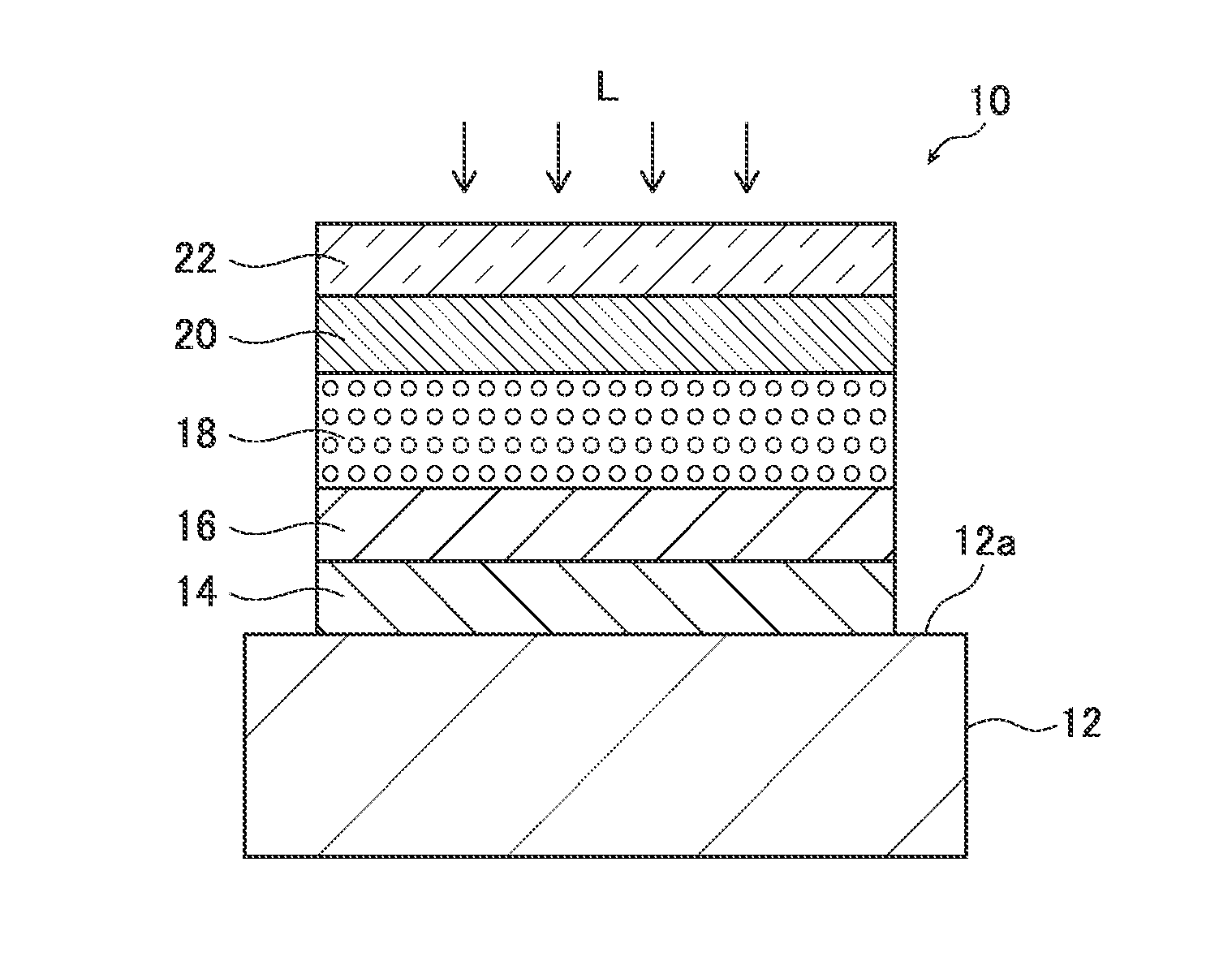
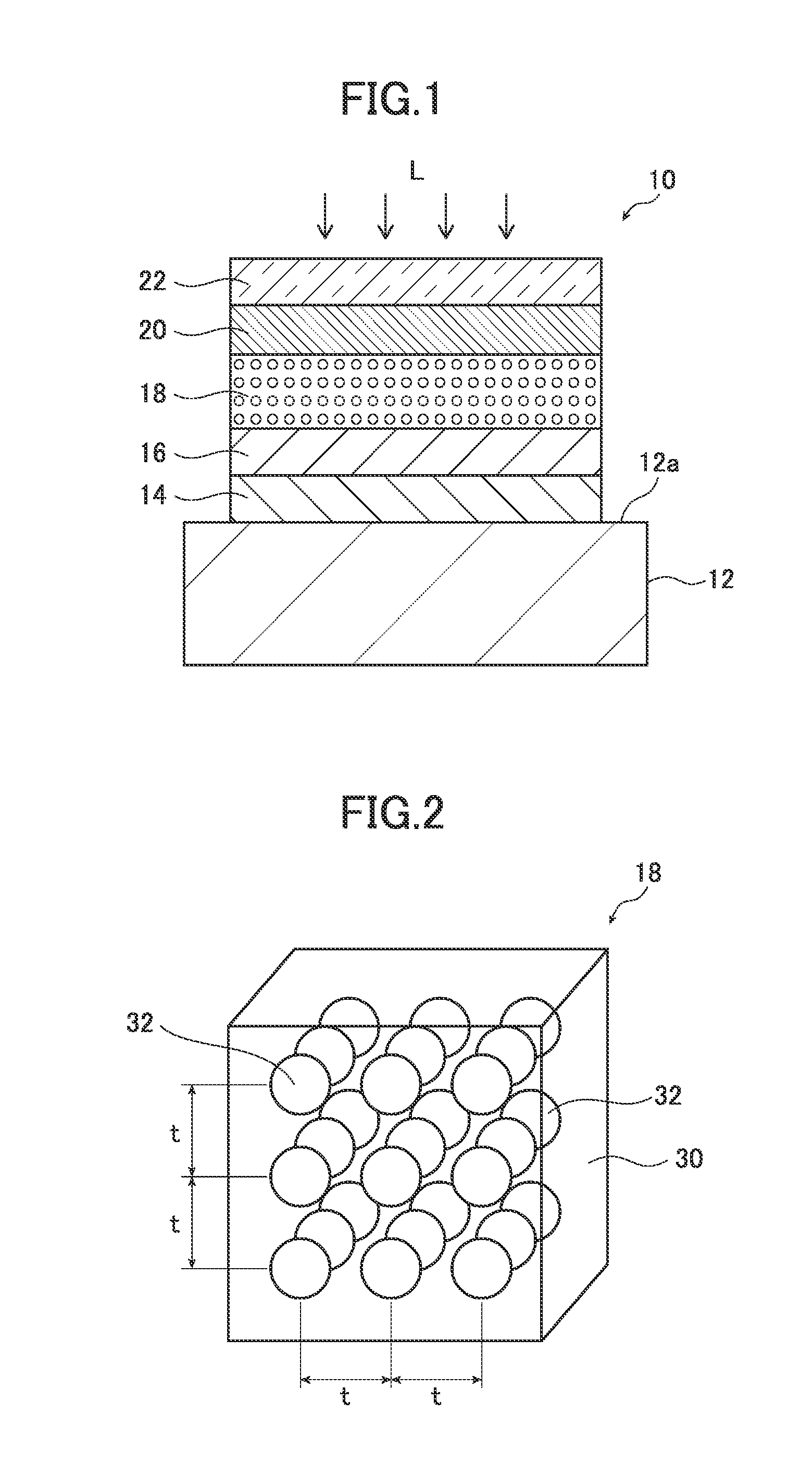
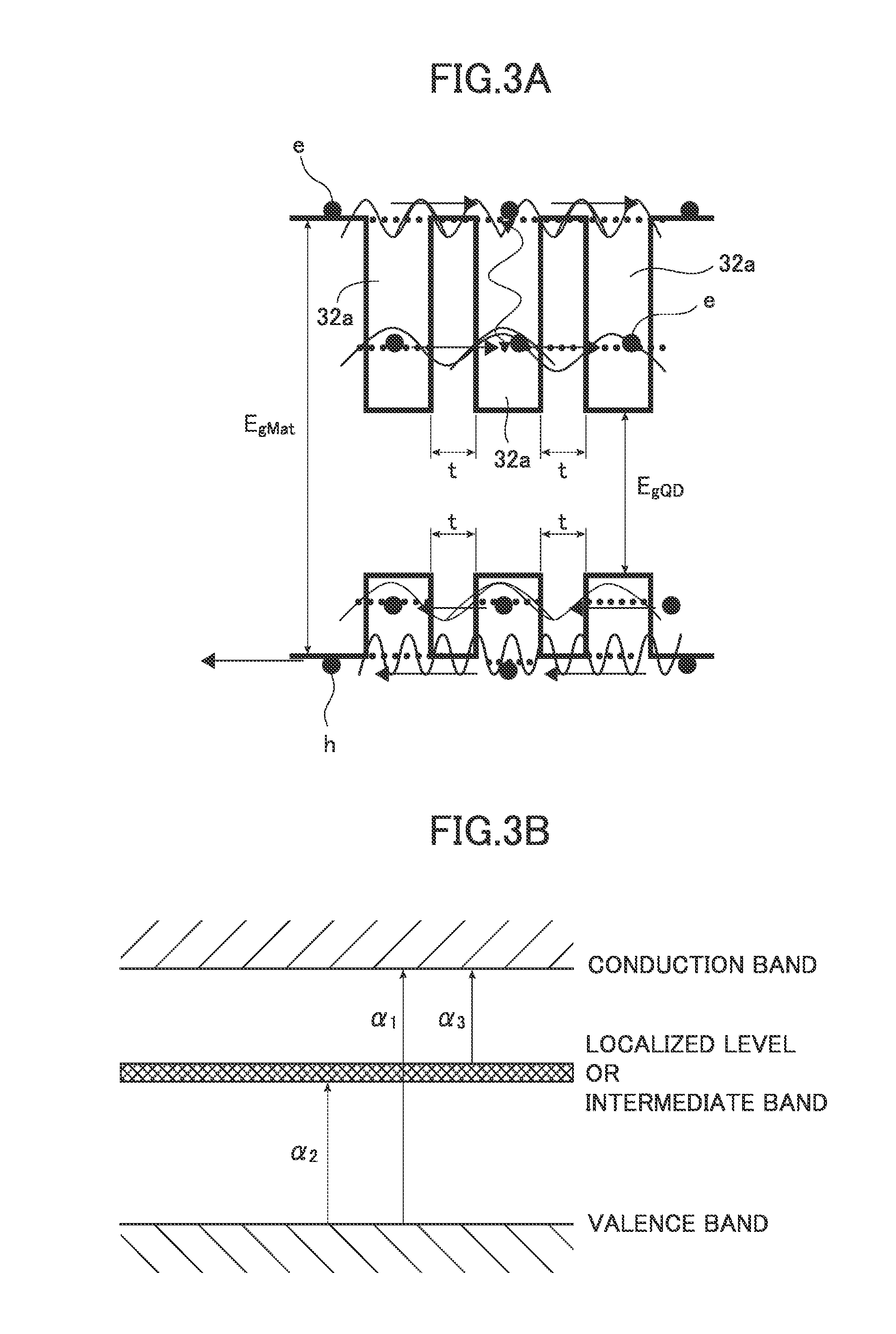
[0052]The solar cell and solar cell production method of the invention will be described below based on preferred embodiments illustrated in the attached drawings.

[0053]The present invention was made based on the following findings obtained by the present inventors.

[0054]Carrier loss due to amorphization of a matrix material is currently thought to be caused by the fact that crystals formed by covalent bond as exemplified by Si and SiC acquire a localized electronic state when the crystals enter a disorderly crystalline state caused by amorphization. It is inferred therefrom that amorphization causes a rapid increase in carrier loss, which in turn makes it impossible to obtain a high energy conversion efficiency. Thus, we thought that use of a material having a carrier conduction track spatially expanding without creating a localized state of electric charge improves conversion efficiency even in disorderly crystalline state caused by amorphization and searched for a material having...


PUM


Abstract

A solar cell capable of restricting carrier loss and yields higher energy conversion efficiency than was conventionally possible and a method of producing a solar cell enabling formation of a light absorbing layer containing quantum dots through a low-temperature process using a coating or printing method requiring no vacuum equipment or complicated apparatuses. The solar cell includes a light absorbing layer containing quantum dots in a matrix layer, and the light absorbing layer is connected to an N-type semiconductor layer on one side and to a P-type semiconductor layer on the other side. In the light absorbing layer, the quantum dots are made of nanocrystalline semiconductor and arranged 3-dimensionally uniformly enough and spaced regularly so that a plurality of wave functions lie on one another between adjacent quantum dots to form intermediate bands. The matrix layer is formed of amorphous IGZO.

Description

BACKGROUND OF THE INVENTION[0001]The present invention relates to a solar cell comprising a light absorbing layer containing quantum dots in a matrix layer formed of amorphous IGZO and a method of manufacturing such solar cell and particularly to a solar cell that achieves a higher conversion efficiency by reducing the carrier loss and a method of manufacturing such solar cell.[0002]Today, intensive researches are being conducted in solar cells. Among the solar cells, a PN-junction solar cell formed by connecting a P-type semiconductor and an N-type semiconductor and a PIN-junction solar cell formed by connecting a P-type semiconductor, an I-type semiconductor, and an N-type semiconductor absorb sunlight having a greater energy than the bandgap (Eg) between a conduction band and a valence band of a component semiconductor, and electrons are excited from the valence band to the conduction band to create positive holes in the valence band, thereby generating electromotive force in the...

Claims


Application Information

Patent Timeline
IPC IPC(8): H01L31/06H01L31/18B82Y20/00B82Y99/00H01L31/0216H01L31/0352
CPCB82Y20/00B82Y30/00Y02E10/548H01L31/075H01L31/035218
Inventor KURAMACHI, TERUHIKOKIKUCHI, MAKOTOHAMA, TAKESHITANAKA, ATSUSHIHOSOYA, YOUICHI
Owner FUJIFILM CORP
Why Eureka
Try Eureka