Sliding contact assembly

a contact assembly and sliding technology, applied in the field of sliding contact assemblies, can solve the problems of insufficient gold flash layer to provide long-term reliable contact resistance without additional protection, the type of plating generates extra costs, and the galvanic hard gold electroplating is also the most expensive technology. , to achieve the effect of reliable and low cos

Inactive Publication Date: 2011-12-08
DELPHI TECH INC
View PDF4 Cites 1 Cited by
  • Summary
  • Abstract
  • Description
  • Claims
  • Application Information

AI Technical Summary

Benefits of technology

[0011]The purpose of the present invention is to solve the above mentioned problem by providing a reliable and low cost solution to build sliding contact assemblies.

Problems solved by technology

Galvanic hard gold electroplated PCBs provide performance and contact reliability for low current applications, but galvanic hard gold electroplating is also the most expensive technology.
This type of plating generates extra costs due to the quantity of gold necessary and due also to the process complexity.
Due to the very low thickness of gold deposited on the contact surface, the gold flash layer is not sufficient to provide long term reliable contact resistance without additional protection.
The main problem with the use of gold flash PCBs is the wear behavior with an extreme sensitivity of gold, even when hardened with cobalt or nickel.
When such gold plated contact sliders are used on gold flash PCBs, the lifetime is too short and some reliability problems may occur.
Such roughness requirements are very difficult to comply with and it increases PCB cost.

Method used


Image

  • Sliding contact assembly
  • Sliding contact assembly

Examples


Embodiment Construction

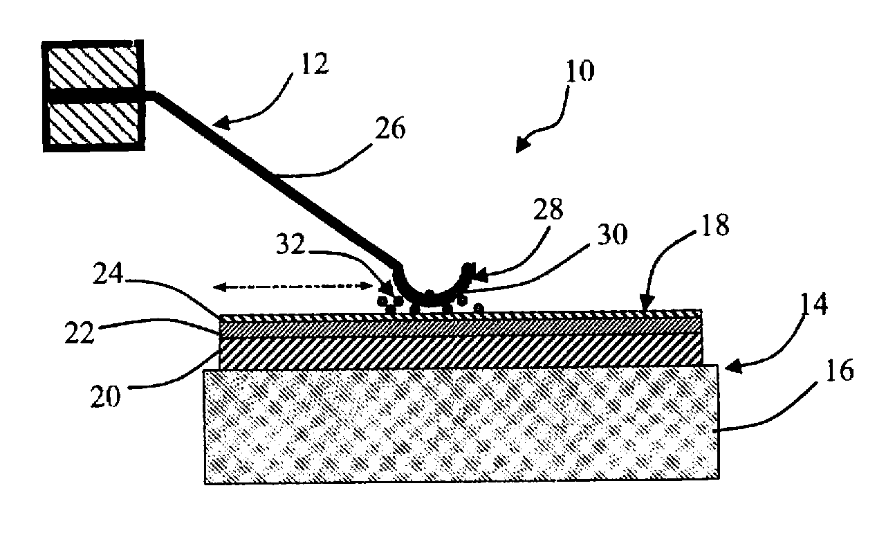
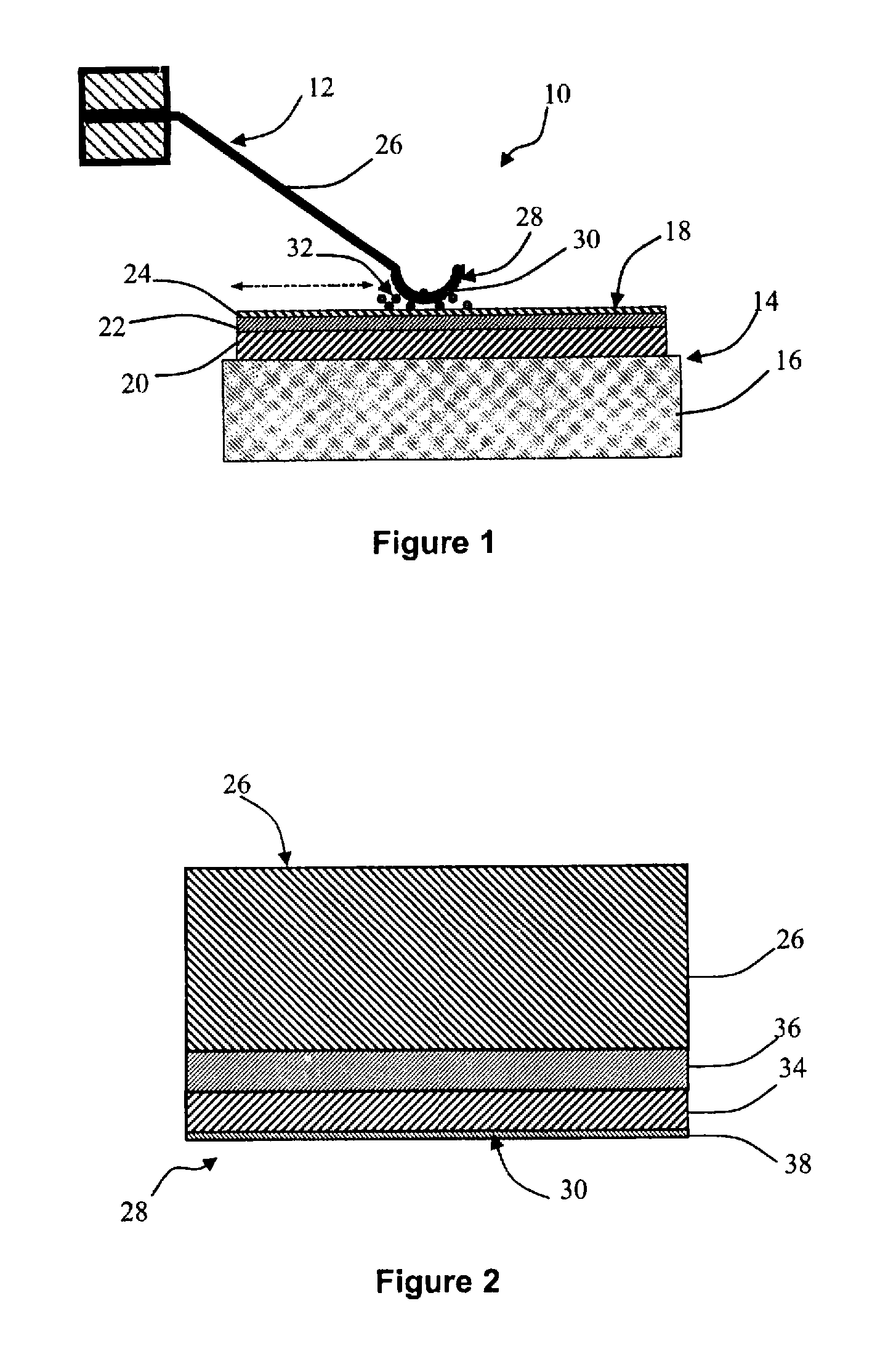
[0033]FIG. 1 shows a sliding contact assembly 10 for low current applications built according to a preferred embodiment of the present invention. The sliding contact assembly 10 includes a movable contact element 12 which is movable along a longitudinal direction X relatively to a printed circuit board (PCB) 14.

[0034]PCB 14 includes a substrate 16 on which is arranged at least one contact pad 18 made of several layers. According to the embodiment shown on FIG. 1, the contact pad 18 is constituted, from the upper surface of the substrate upwards of:[0035]a base layer 20 of copper, for example 35 μm thick,[0036]an intermediate layer 22 of nickel, preferably 3 to 6 μm thick, and[0037]an external layer 24 essentially made of gold, preferably 0.15 μm thick or less.

[0038]As may be seen, the external layer 24 of gold is made very thin, compared to the two other layers. It may be made of gold alloy hardened with cobalt (AuCo) or Nickel (AuNi).

[0039]Advantageously, the external layer 24 is d...


PUM

PropertyMeasurementUnit
thicknessaaaaaaaaaa
thicknessaaaaaaaaaa
thicknessaaaaaaaaaa

Abstract

A sliding contact assembly includes a printed circuit board having a substrate on which is arranged at least one contact pad. The at least one contact pad is made of several layers including a thin external layer essentially made of gold. The gold layer is deposited on the at least one contact pad through a gold flash type process. The assembly also includes a movable contact element including a support member. The support member has a contact surface provided with a protective coating and the contact surface is biased against the said contact pad when the movable contact element is moved in relation to the contact pad. The protective coating includes a palladium alloy layer. Methods to manufacture a sliding contact assembly are also presented.

Description

CROSS-REFERENCE TO RELATED APPLICATION[0001]This application claims the benefit under 35 U.S.C. §371 of published PCT Patent Publication No. PCT / EP2010 / 051249, filed on 2 Feb. 2010, which claims priority to EP 09152117.9 filed on 5 Feb. 2009, the entire disclosure of which is hereby respectively incorporated by reference herein.TECHNICAL FIELD[0002]The present invention relates generally to sliding contact assemblies for low current applications.BACKGROUND OF INVENTION[0003]The present invention relates more particularly to a sliding contact assembly to be implemented in a vehicle. One such example is in the column integrated module (CIM) arranged on the steering column of the vehicle used for electrical connection of switch devices.[0004]Automotive suppliers have used printed circuit boards (PCB) having gold plating pads as direct contact interface for low current sliding contacts. Several gold plating processes are available on the market, providing various wear behavior.[0005]Gal...

Claims


Application Information

Patent Timeline
Patent Type & Authority Applications(United States)
IPC IPC(8): H05K1/09H01R9/00
CPCH01H1/025H01H1/403H01H15/04Y10T29/49147H05K3/244H05K3/325H01H15/06
Inventor LE SOLLEU, JEAN-PIERRE
Owner DELPHI TECH INC
Why Eureka
Try Eureka