Method of crystallizing silicon thin film and method of manufacturing silicon thin-film transistor device
- Summary
- Abstract
- Description
- Claims
- Application Information
AI Technical Summary
Benefits of technology
Problems solved by technology
Method used
Image

Examples
embodiment
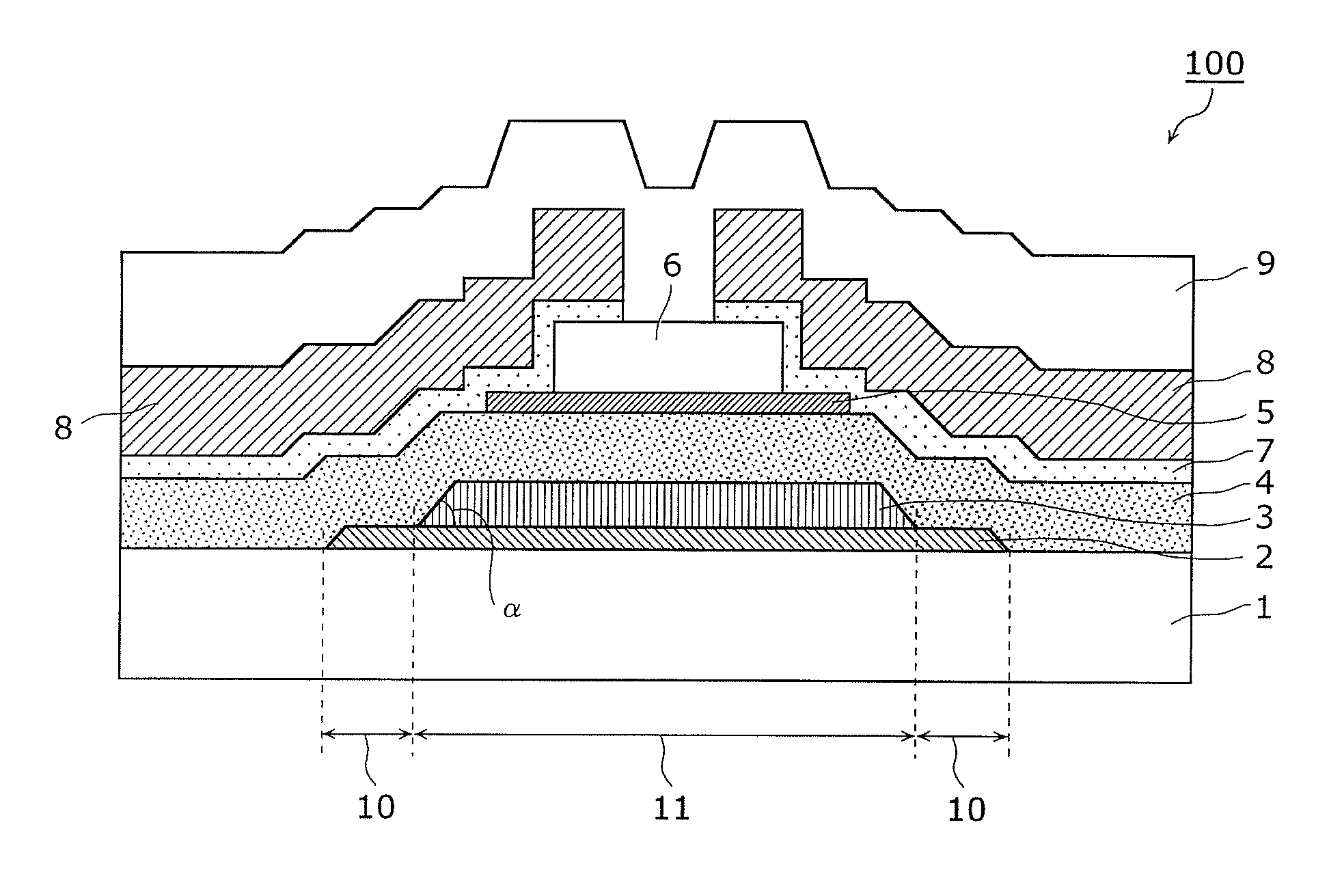
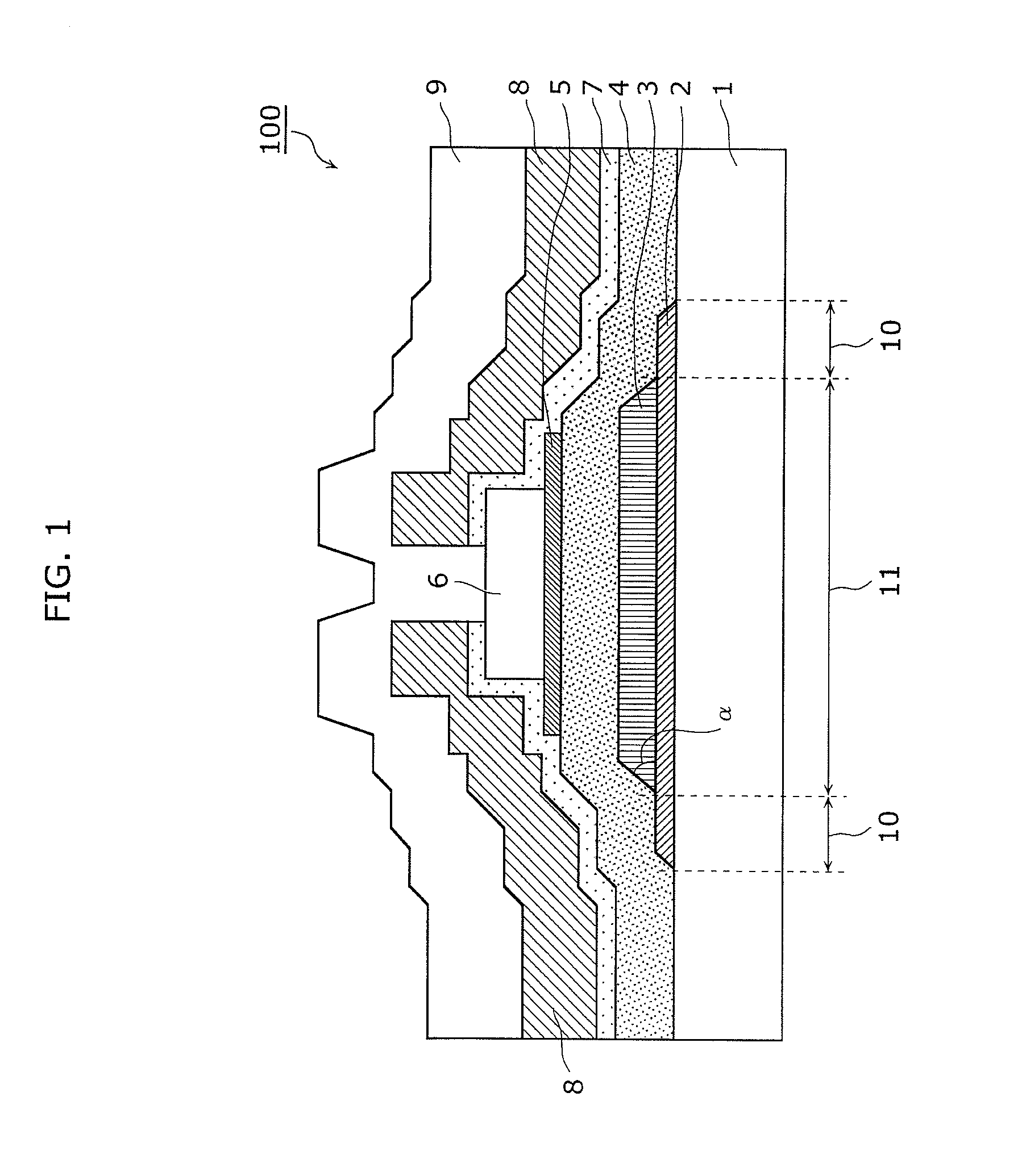
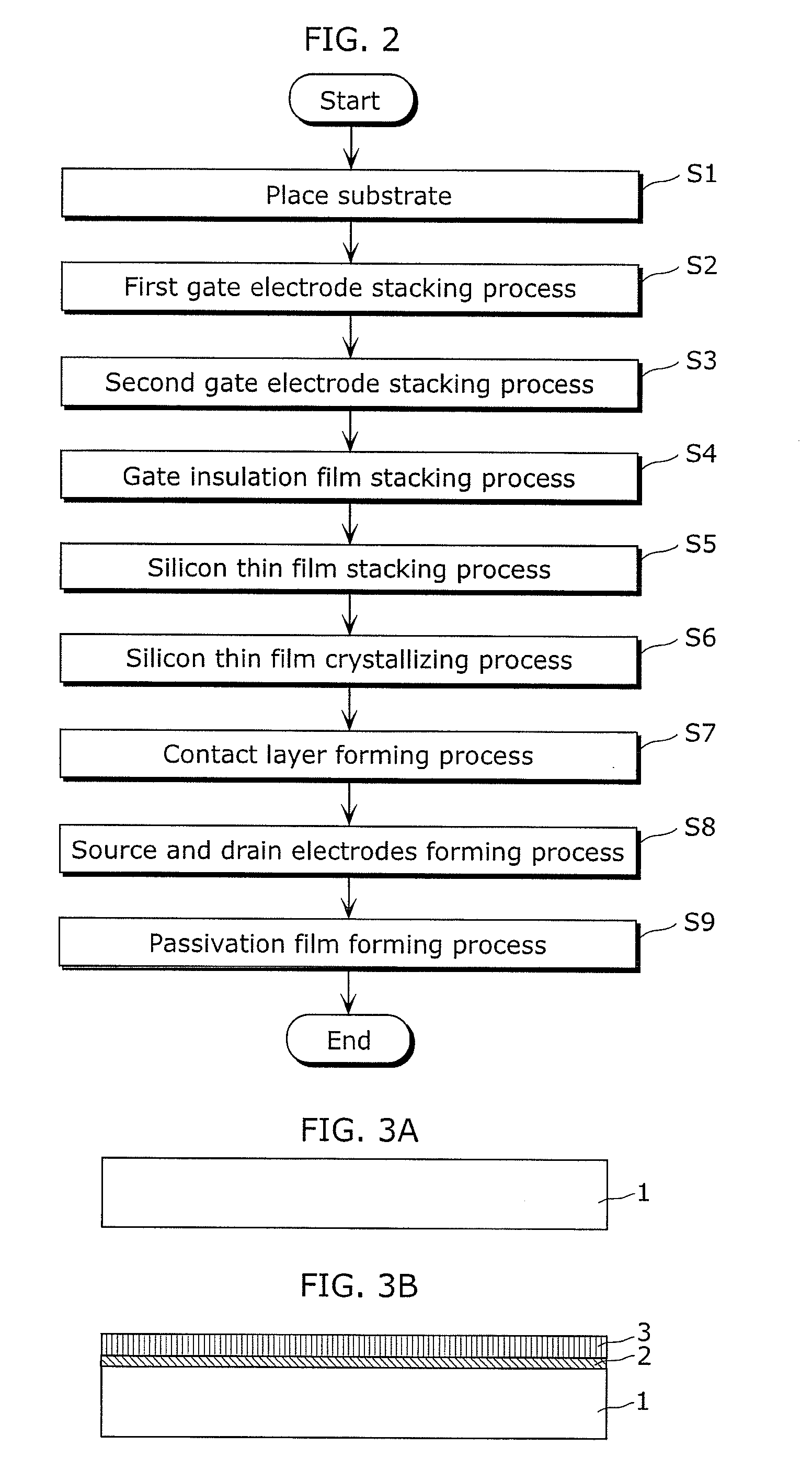
[0088]The FIG. 1 is a cross-sectional view schematically illustrating a configuration of a silicon TFT device according to an embodiment of the present invention. A silicon TFT device 100 in the diagram is a thin-film transistor device of a bottom-gate type, and includes: a first gate electrode 2; a second gate electrode 3; a gate insulation film 4; a crystalline silicon thin film 5; an insulation film 6; a pair of contact layers 7; a pair of source and drain electrodes 8; and a passivation film 9, which are sequentially stacked on a substrate 1.
[0089]The substrate 1 is a substrate formed of a transparent glass or quartz, for example.
[0090]The first gate electrode 2 includes, for example, a metal such as Cu (copper), Al (aluminum), and the like, or an alloy including Cu (copper), Al (aluminum), and the like, and is formed on the substrate 1 to have a thickness of 50 nm, for example. The first gate electrode 2 has a first reflectivity of a metal included in the first gate electrode 2...
example
[0145]FIG. 8A and FIG. 8B are diagrams each of which illustrates a model structure and a parameter used for calculation in the example. Here, k is an attenuation coefficient.
[0146]In the model structure shown in FIG. 8A, a glass is placed as a substrate, a SiN film having a thickness of 150 nm is placed on the glass, and a metal film having a thickness of 50 nm is placed on the SiN film. A SiO2 film having a variable thickness is placed on the SiN film to cover the metal film, and an a-Si film is placed on the SiO2 film. An air layer having a refraction index of 1 is provided above the a-Si film. Here, this model structure is a modelization of a structure of the bottom-gate TFT according to the embodiment shown in (a) in FIG. 4. Here, the SiN film corresponds to the substrate 1 shown in FIG. 4 and the metal film corresponds to the first gate electrode 2. The SiO2 film corresponds to the gate insulation film 4 and the a-Si film corresponds to the noncrystalline silicon thin film 5a. ...
PUM
 Abstract
Description
Claims
Application Information
 - R&D Engineer
- R&D Manager
- IP Professional
- Industry Leading Data Capabilities
- Powerful AI technology
- Patent DNA Extraction
Browse by: Latest US Patents, China's latest patents, Technical Efficacy Thesaurus, Application Domain, Technology Topic.
© 2024 PatSnap. All rights reserved.Legal|Privacy policy|Modern Slavery Act Transparency Statement|Sitemap