Electrophotographic photoconductor, image forming apparatus, and process cartridge
a photoconductor and electrotax technology, applied in the field of electrotax photoconductor, image forming apparatus, and process cartridges, can solve the problems of poor mechanical resistance, inorganic photoconductors, scratches, etc., and achieve the effect of achieving mechanical resistance and high releasing ability, and stably outputting high-quality images
- Summary
- Abstract
- Description
- Claims
- Application Information
AI Technical Summary
Benefits of technology
Problems solved by technology
Method used
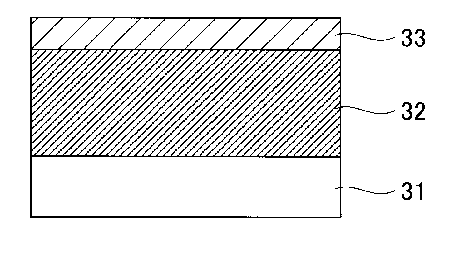
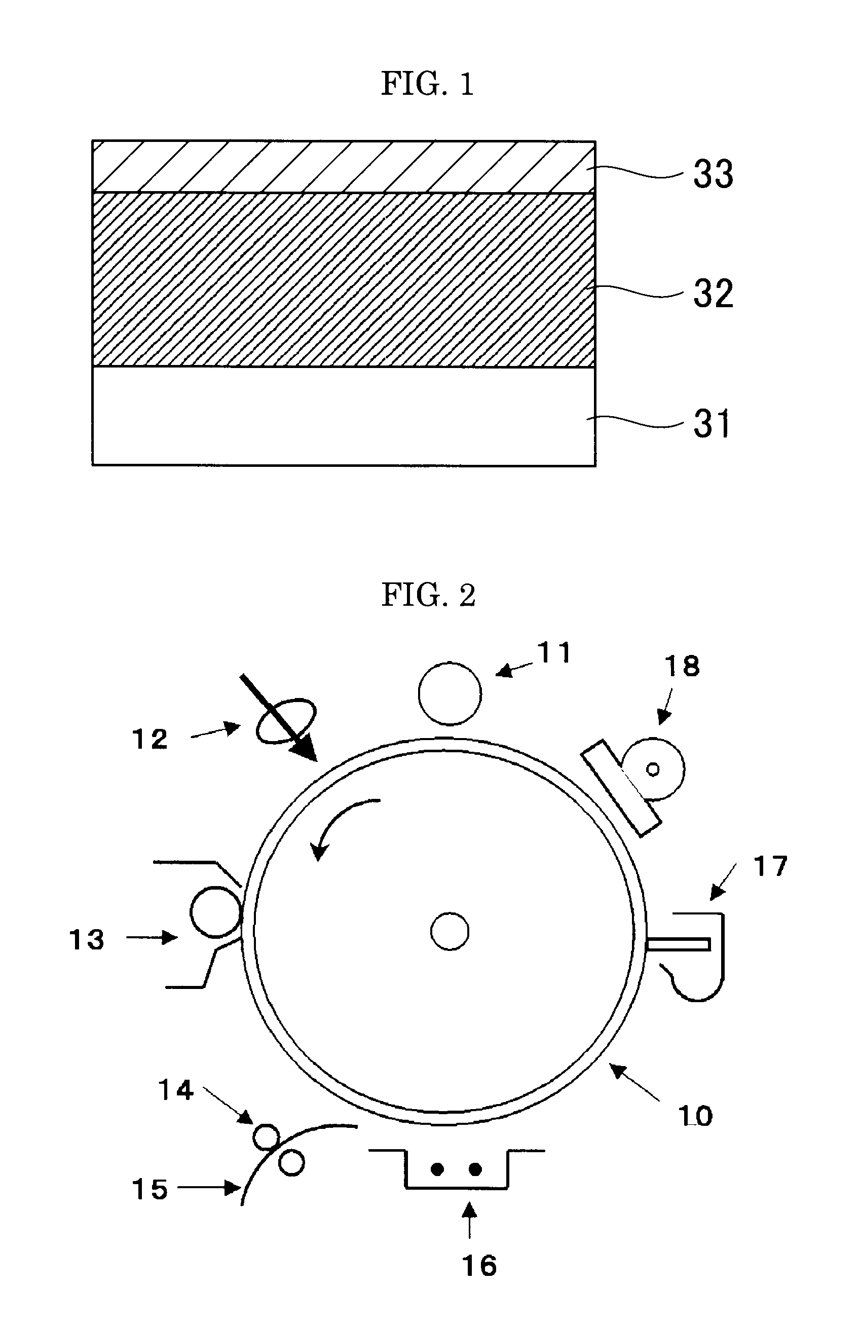
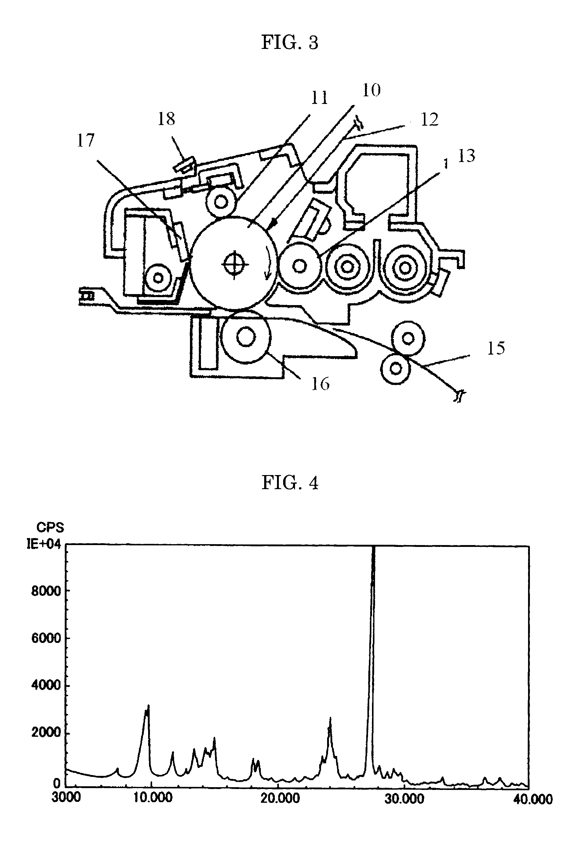
Image

Examples
synthesis example 1
Synthesis of Titanyl Phthalocyanine Crystal
[0144]A synthesis method of a titanyl phthalocyanine used in the present invention will be explained. The synthesis was carried out based on the method described in JP-A No. 2004-83859. Specifically, 292 parts of 1,3-diiminoisoindoline and 1,800 parts of sulfolane were mixed, and to the mixture 204 parts of titanium tetrabutoxide was added dropwose under the stream of nitrogen. After the dropwise addition was completed, the temperature of the resulting mixture was gradually elevated to 180° C., and the mixture was allowed to react for 5 hours with stirring while maintaining the temperature at 170° C. to 180° C. After the completion of the reaction, the reaction mixture was left to stand for cooling, and the resulting precipitate was separated by filtration. The separated precipitate was washed with chloroform until the powder of the precipitate became the color of blue, followed by washing with methanol a few times, further washing with ho...
PUM
| Property | Measurement | Unit |
|---|---|---|
| volume resistivity | aaaaa | aaaaa |
| thickness | aaaaa | aaaaa |
| thickness | aaaaa | aaaaa |
Abstract
Description
Claims
Application Information