
Making of a microelectronic device including a monocrystalline silicon nems component and a transistor the gate of which is made in the same layer as the mobile structure of this component

Active Publication Date: 2012-01-12
COMMISSARIAT A LENERGIE ATOMIQUE ET AUX ENERGIES ALTERNATIVES
View PDF1 Cites 3 Cited by
  • Summary
  • Abstract
  • Description
  • Claims
  • Application Information

AI Technical Summary

Benefits of technology

[0055]The number of steps of the method for connecting these components can thus be reduced, while limiting the stray capacitance phenomena between the electromechanical component and the processing circuit connected to this component.
[0057]By restricting the stray capacitances, it may be possible to provide a lower transistor gain, and thus to reduce consumption.

Problems solved by technology

A drawback common to these different approaches is related to the number of manufacturing steps required to make the MEMS component and CMOS circuit.
However, the use of polycrystalline silicon for making the mobile structure of a MEMS restricts the mechanical performances as well as the reliability of this MEMS structure.
The total SiGe removal is difficult to achieve when the critical dimension of the SiGe area is important, which imposes to make low channel size transistors.

Method used


Image

  • Making of a microelectronic device including a monocrystalline silicon nems component and a transistor the gate of which is made in the same layer as the mobile structure of this component
  • Making of a microelectronic device including a monocrystalline silicon nems component and a transistor the gate of which is made in the same layer as the mobile structure of this component
  • Making of a microelectronic device including a monocrystalline silicon nems component and a transistor the gate of which is made in the same layer as the mobile structure of this component

Examples


Embodiment Construction

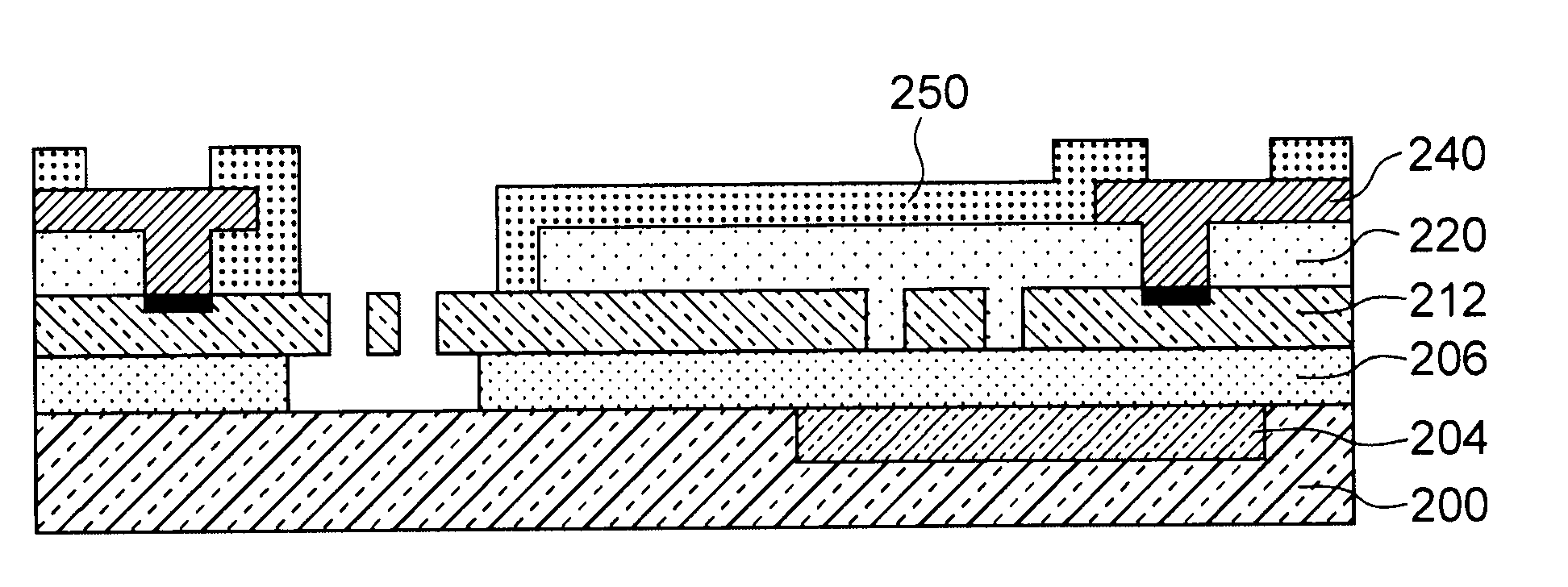
[0017]The invention relates to a method for making a microelectronic device comprising, on a same substrate, at least one electro-mechanical component provided with a mobile structure of a monocrystalline semi-conductor material and means for actuating and / or detecting the mobile structure, and with at least one transistor,

[0018]the method comprising the following steps of:

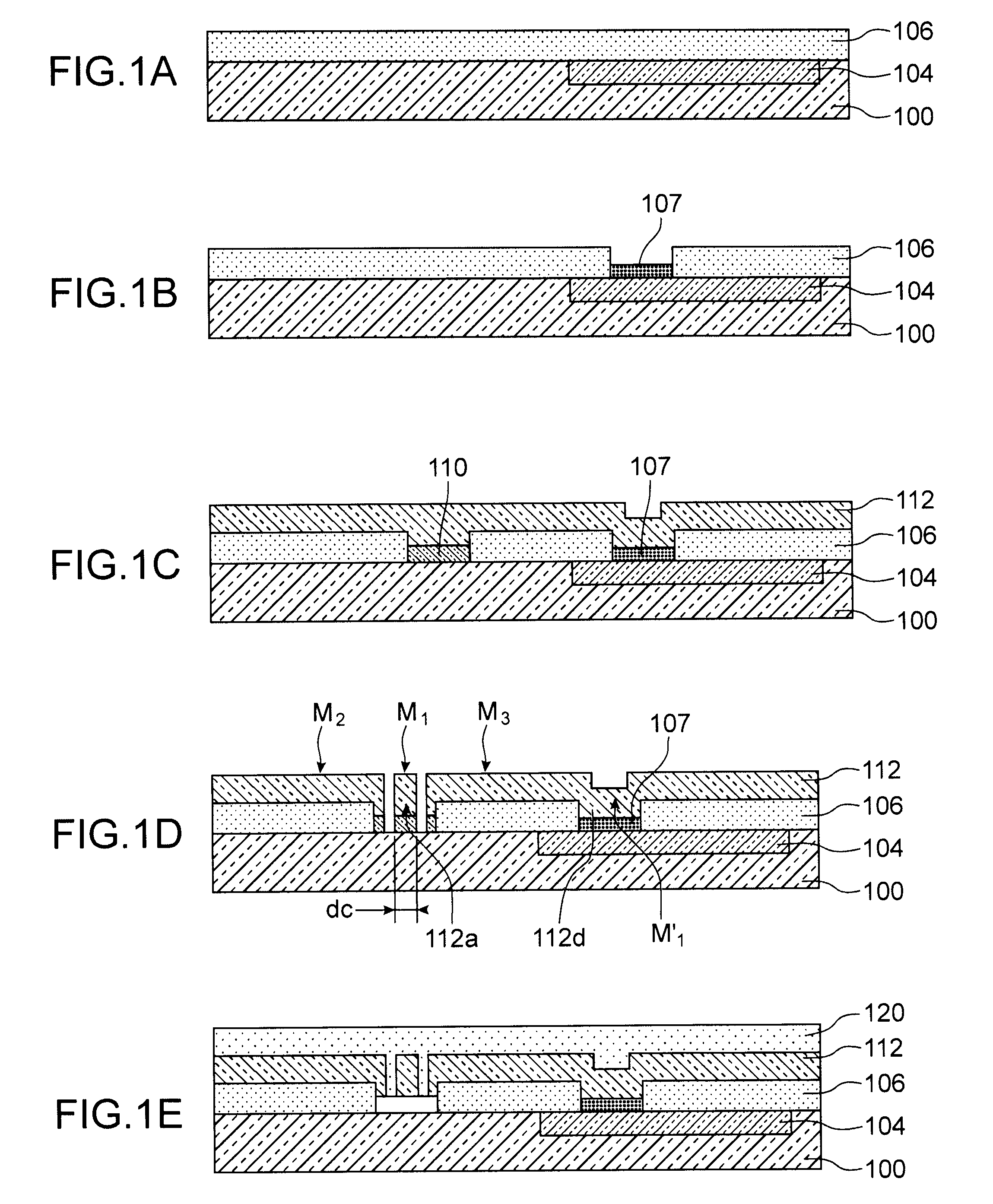
[0019]a) providing a substrate provided with at least one first semi-conducting layer including at least one given region wherein a channel area of the transistor is provided, an insulating layer covering the first semi-conducting layer,

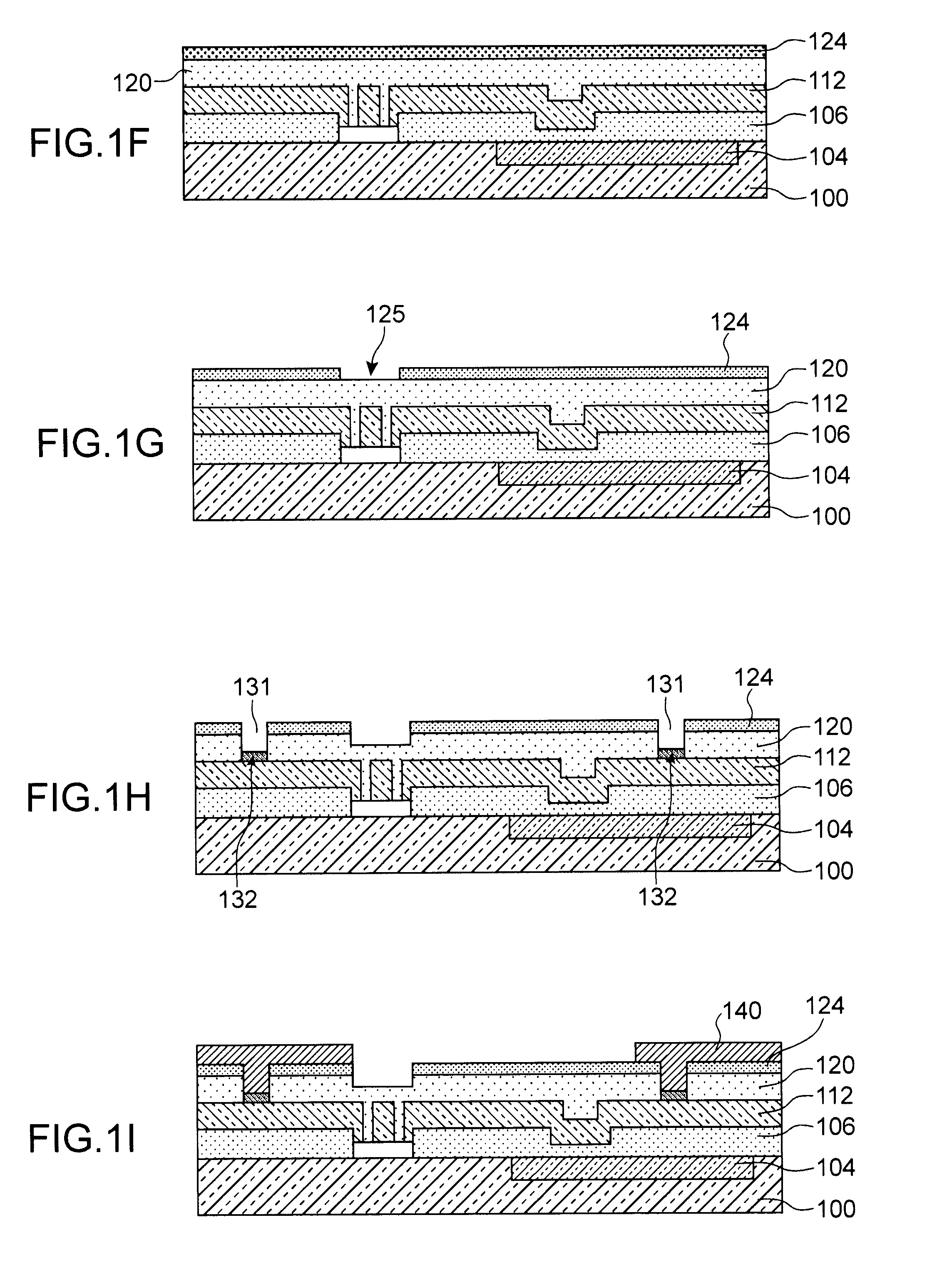
[0020]b) etching a second semi-conducting layer based on a given semi-conductor material, lying on said insulating layer covering said first semi-conducting layer, the etching being provided so as to form at least one pattern of said mobile structure of the component in an area of monocrystalline semi-conductor material of the material of the second semi-conducting layer, and at le...


PUM


Abstract

A method for making a microelectronic device including, on a same substrate, at least one electro-mechanical component including a mobile structure of a monocrystalline semi-conductor material and a mechanism actuating and / or detecting the mobile structure, and with at least one transistor. The method a) provides a substrate including at least one first semi-conducting layer including at least one region in which a channel area of the transistor is provided, b) etches a second semi-conducting layer based on a given semi-conductor material, lying on an insulating layer placed on the first semi-conducting layer, to form at least one pattern of the mobile structure of the component in an area of monocrystalline semi-conductor material of the second semi-conducting layer, and at least one pattern of gate of the transistor on a gate dielectric area located facing the given region.

Description

TECHNICAL FIELD[0001]The present invention relates to the field of microelectronic devices provided with at least one NEMS (Nano Electro-Mechanical Systems) and / or MEMS (Micro Electro Mechanical Systems) component cointegrated on a same substrate with at least one transistor.[0002]The invention allows to form a mobile structure of a MEMS or NEMS component in a monocrystalline Si, and a transistor from a same semi-conducting layer, and provides improvements in particular in terms of the number of manufacturing method steps required to make the MEMS component and the electronic circuit.PRIOR ART[0003]It is known to integrate on a same substrate, a NEMS and / or MEMS structure with one or more transistors of a CMOS circuit is known.[0004]For this, there are different methods, which have been, for example, described in document: “On Integrated CMOS-MEMS System-on-Chip”, Soumik Ghosh et Magdy Bayoumi, conference IEEE-NEWCAS 2005, pp. 31-34.[0005]One approach called “pre-CMOS” specifies mak...

Claims


Application Information

Patent Timeline
IPC IPC(8): H01L21/8234
CPCB81C2203/0735B81C1/00246
Inventor OLLIER, ERICBERTHELOT, AUDREY
Owner COMMISSARIAT A LENERGIE ATOMIQUE ET AUX ENERGIES ALTERNATIVES
Learn More