Semiconductor device and method for fabricating the same

a technology of semiconductor devices and dram cells, which is applied in the direction of semiconductor devices, electrical equipment, transistors, etc., can solve the problems of increasing the number of dram cells per given wafer size, increasing the parasitic capacitance in the bit line, etc., and achieves the effect of reducing the parasite capacitance and reducing the leakage curren

Active Publication Date: 2012-01-19
SK HYNIX INC
View PDF7 Cites 24 Cited by
  • Summary
  • Abstract
  • Description
  • Claims
  • Application Information

AI Technical Summary

Benefits of technology

[0006]Various embodiments of the invention are directed to providing a semiconductor device and a method for fabricating the same that includes a bit line spacer formed with an oxide film to reduce a parasite capacitance, a storage node contact formed with a line type to secure a patterning margin and a storage node contact plug formed with polysilicon having a different concentration, thereby reducing leakage current.

Problems solved by technology

Recently, although a semiconductor memory device, specifically, a Dynamic Random Access Memory (DRAM), is required to have large capacity, the increase in the number of DRAM cell per a given wafer size has been limited due to a restriction in the increase of the chip size.
However, since the nitride film has a high dielectric constant, a parasitic capacitance is increased in the bit line.
However, when a storage node contact hole is etched, an overlay process is employed to decrease contact resistance between a storage electrode and a source region.

Method used


Image

  • Semiconductor device and method for fabricating the same
  • Semiconductor device and method for fabricating the same
  • Semiconductor device and method for fabricating the same

Examples


Embodiment Construction

[0030]The present invention will be described in detail with reference to the attached drawings.

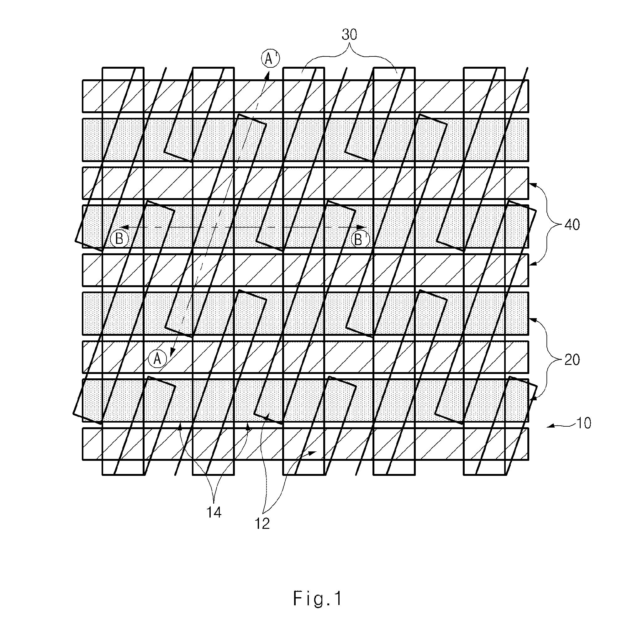
[0031]FIG. 1 is a plan view illustrating a semiconductor device according to an embodiment of the present invention.

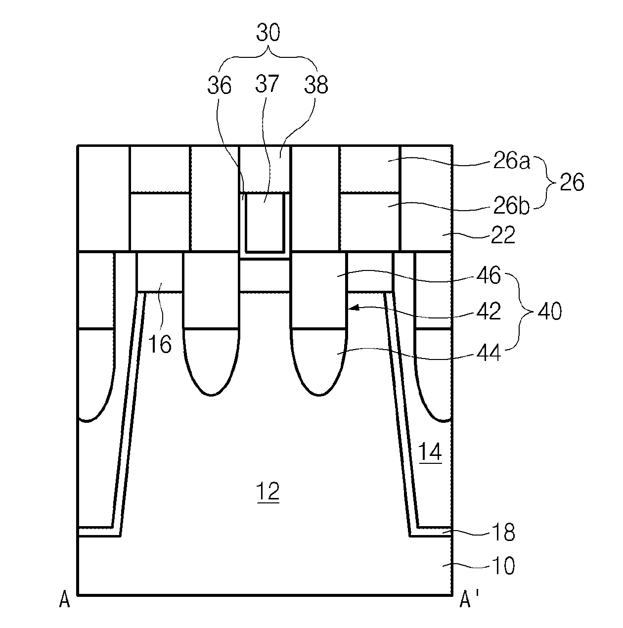
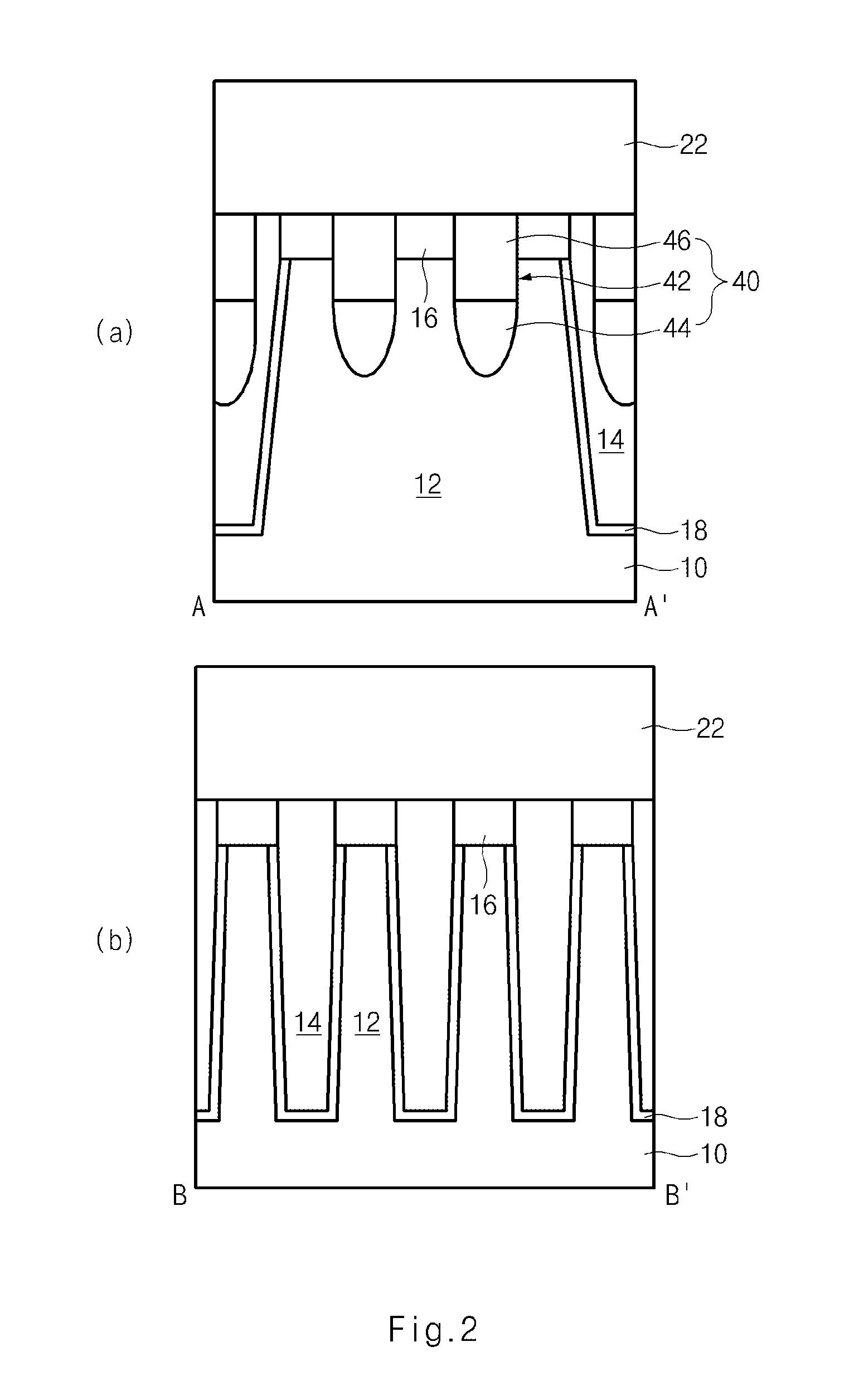
[0032]Referring to FIG. 1, a device isolation film 14 that defines an active region 12 is disposed in a semiconductor substrate 10. A gate 40 is formed passing over the active region 12 along a horizontal direction. A bit line 30 is formed passing over the active region 12 along a vertical direction. Along a direction parallel to the gate 40, a storage node contact 20 having a line type is disposed in a space between the adjacent gates 40.

[0033]The gate 40 is a buried gate buried in a recess defined in the semiconductor substrate 10. The bit line 30 is formed by a damascene process. In the damascene process, the storage node contacts 20 are separated from each other.

[0034]FIGS. 2 to 9 are cross-sectional diagrams illustrating a method for fabricating a semiconductor device a...


PUM

PropertyMeasurementUnit
conductiveaaaaaaaaaa
thicknessaaaaaaaaaa
depthaaaaaaaaaa

Abstract

A semiconductor device comprises: a semiconductor substrate including an active region defined as a device isolation film; a bit line hole disposed over the top portion of the semiconductor substrate; an oxide film disposed at sidewalls of the bit line hole; and a bit line conductive layer buried in the bit line hole including the oxide film. A bit line spacer is formed with an oxide film, thereby reducing a parasitic capacitance. A storage node contact is formed to have a line type, thereby securing a patterning margin. A storage node contact plug is formed with polysilicon having a different concentration, thereby reducing leakage current.

Description

CROSS-REFERENCE TO RELATED APPLICATION[0001]The priority of Korean patent application No. 10-2010-0068371 filed on Jul. 15, 2010, the disclosure of which is hereby incorporated in its entirety by reference, is claimed.BACKGROUND OF THE INVENTION[0002]An embodiment of the present invention relates to a semiconductor device, and more specifically, to a semiconductor device and method for manufacturing the same including a bit line.[0003]Recently, although a semiconductor memory device, specifically, a Dynamic Random Access Memory (DRAM), is required to have large capacity, the increase in the number of DRAM cell per a given wafer size has been limited due to a restriction in the increase of the chip size. If the chip size is increased, the number of chips per wafer is decreased and the productivity of the device is reduced. As a result, the cell layout has been recently changed to reduce the cell area and research into integrating more memory cells into one wafer has been ongoing.[000...

Claims


Application Information

Patent Timeline
Patent Type & Authority Applications(United States)
IPC IPC(8): H01L27/108H01L21/8242
CPCH01L27/10823H01L27/10867H01L27/10882H01L27/10888H01L21/28008H01L27/10885H10B12/34H10B12/0385H10B12/485H10B12/482H10B12/48
Inventor KWON, SE IN
Owner SK HYNIX INC
Why Eureka
Try Eureka