Structure And Method For Dual Work Function Metal Gate CMOS With Selective Capping

Active Publication Date: 2012-01-26
TEXAS INSTR INC
View PDF7 Cites 35 Cited by
  • Summary
  • Abstract
  • Description
  • Claims
  • Application Information

AI Technical Summary

Benefits of technology

[0009]An advantage of the invention is providing a CMOS device with the desired band edge work functions for NMOS and PMOS transistors by controlling the oxygen concentration in

Problems solved by technology

The use of doped polysilicon gates becomes problematic, however, as the dimensions of gates and gate insulators are reduced.
The manufacture of semiconductor devices having independently adjustable dual work function metal gates has been troublesome, however.
It is challenging, however, to find such metals.
This can result in the same type of Vt offset problem encountered for dope

Method used


Image

  • Structure And Method For Dual Work Function Metal Gate CMOS With Selective Capping
  • Structure And Method For Dual Work Function Metal Gate CMOS With Selective Capping
  • Structure And Method For Dual Work Function Metal Gate CMOS With Selective Capping

Examples


Embodiment Construction

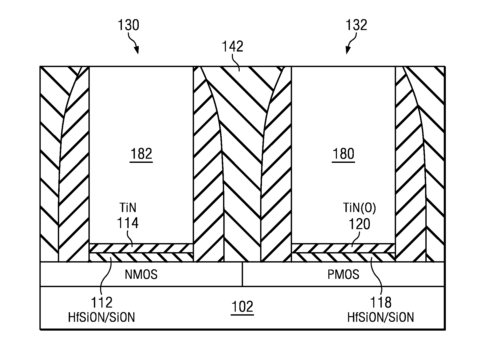
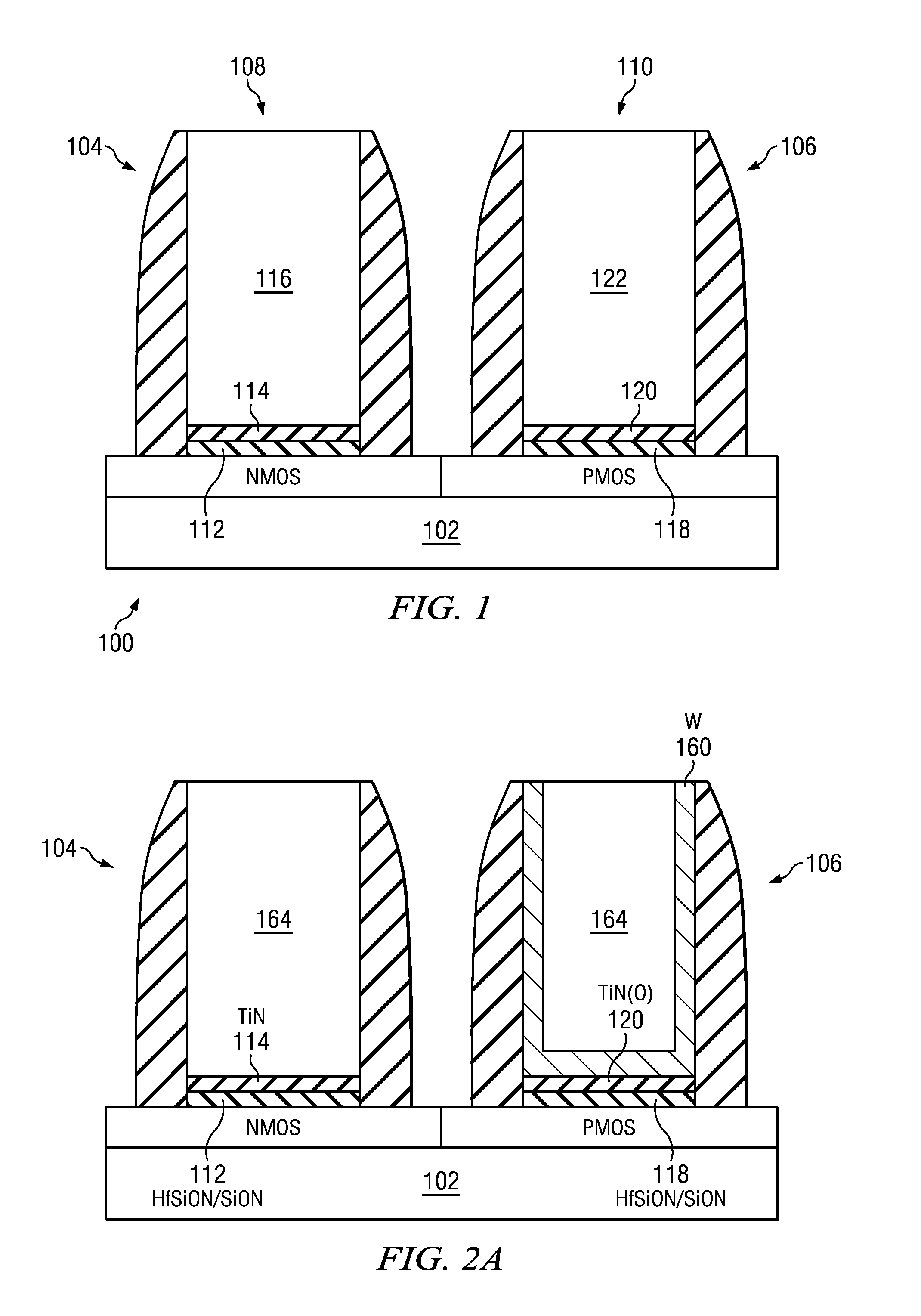
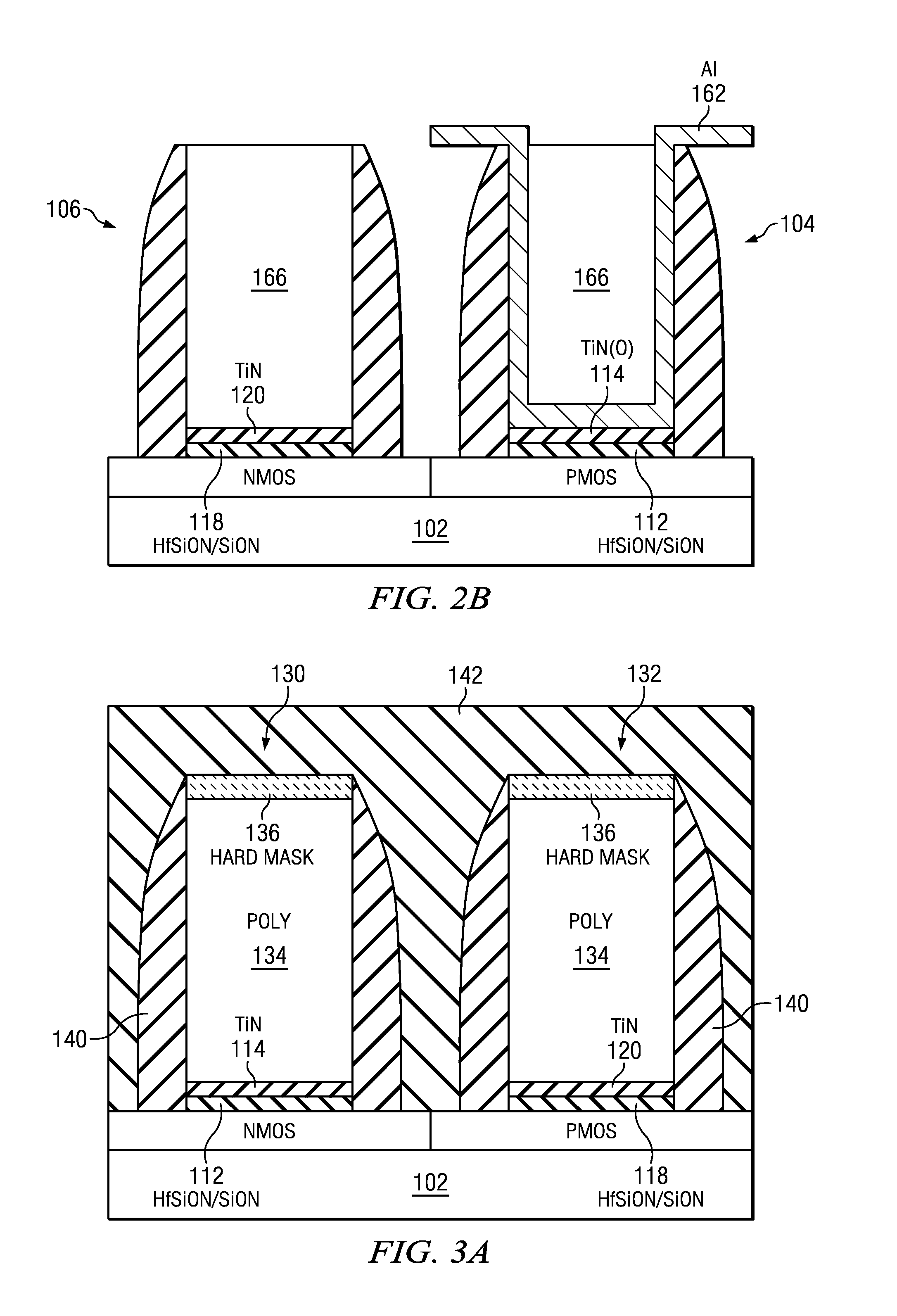
[0016]Oxygen control in metal gate stacks is crucial in obtaining the desired band edge work functions. Oxygen at the interface between the metal gate and the dielectric is beneficial for obtaining high work function in PMOS devices. The opposite is true for NMOS where the ability to obtain low work function depends in part on the ability to denude the metal gate / dielectric interface of oxygen while at the same time incorporating a low work function metal at the interface. The invention provides a device and method for accomplishing oxygen control in metal gate stacks while incorporating a low work function metal at the interface in NMOS transistors.

[0017]FIG. 1 illustrates a CMOS device 100 according to the invention. Device 100 includes an NMOS transistor 104 and a PMOS transistor 106 located at the surface of a semiconductor body 102. Semiconductor body 102 may, for example, comprise a silicon substrate with or without epitaxial layers formed thereon. Alternative examples include...


PUM


Abstract

A CMOS device having an NMOS transistor with a metal gate electrode comprising a mid-gap metal with a low work function/high oxygen affinity cap and a PMOS transistor with a metal gate electrode comprising a mid gap metal with a high work function/low oxygen affinity cap and method of forming.

Description

[0001]This application claims the benefit of U.S. Provisional Application No. 61 / 294,661, filed Jan. 13, 2010.FIELD OF THE INVENTION[0002]The invention is generally related to the field of semiconductor devices and more specifically to dual work function metal gates in CMOS applications.BACKGROUND OF THE INVENTION[0003]The ability to dope polysilicon gates to different degrees allows one to adjust the work function of gate electrode materials to particular types of metal oxide semiconductor (MOS) transistors. It is desirable to adjust the work function of a gate electrode (hereinafter, the gate), to be close to either the conduction band or the valence band of silicon, because this reduces the threshold voltage (Vt) of the transistor, thereby facilitating a high drive current at low operating voltages. For instance, dual work function gates created using doped polysilicon are advantageously used in semiconductor devices, such as complementary metal oxide semiconductor (CMOS) transis...

Claims


Application Information

Patent Timeline
IPC IPC(8): H01L27/092H01L21/28
CPCH01L21/28079H01L21/28088H01L21/823842H01L21/823857H01L21/283H01L29/4966H01L29/517H01L29/518H01L29/66545H01L29/4958
Inventor CHAMBERS, JAMES JOSEPHNIIMI, HIROAKI
Owner TEXAS INSTR INC
Why Eureka
Try Eureka