

Method and system for electronic spatial filtering of spectral reflectometer optical signals
a technology of optical signals and electronic spatial filtering, applied in the field of spectral reflectometry, can solve the problems of prohibitively expensive, poor signal contrast, and addition of additional hardwar
- Summary
- Abstract
- Description
- Claims
- Application Information
AI Technical Summary
Benefits of technology
Problems solved by technology
Method used
Image

Examples
Embodiment Construction
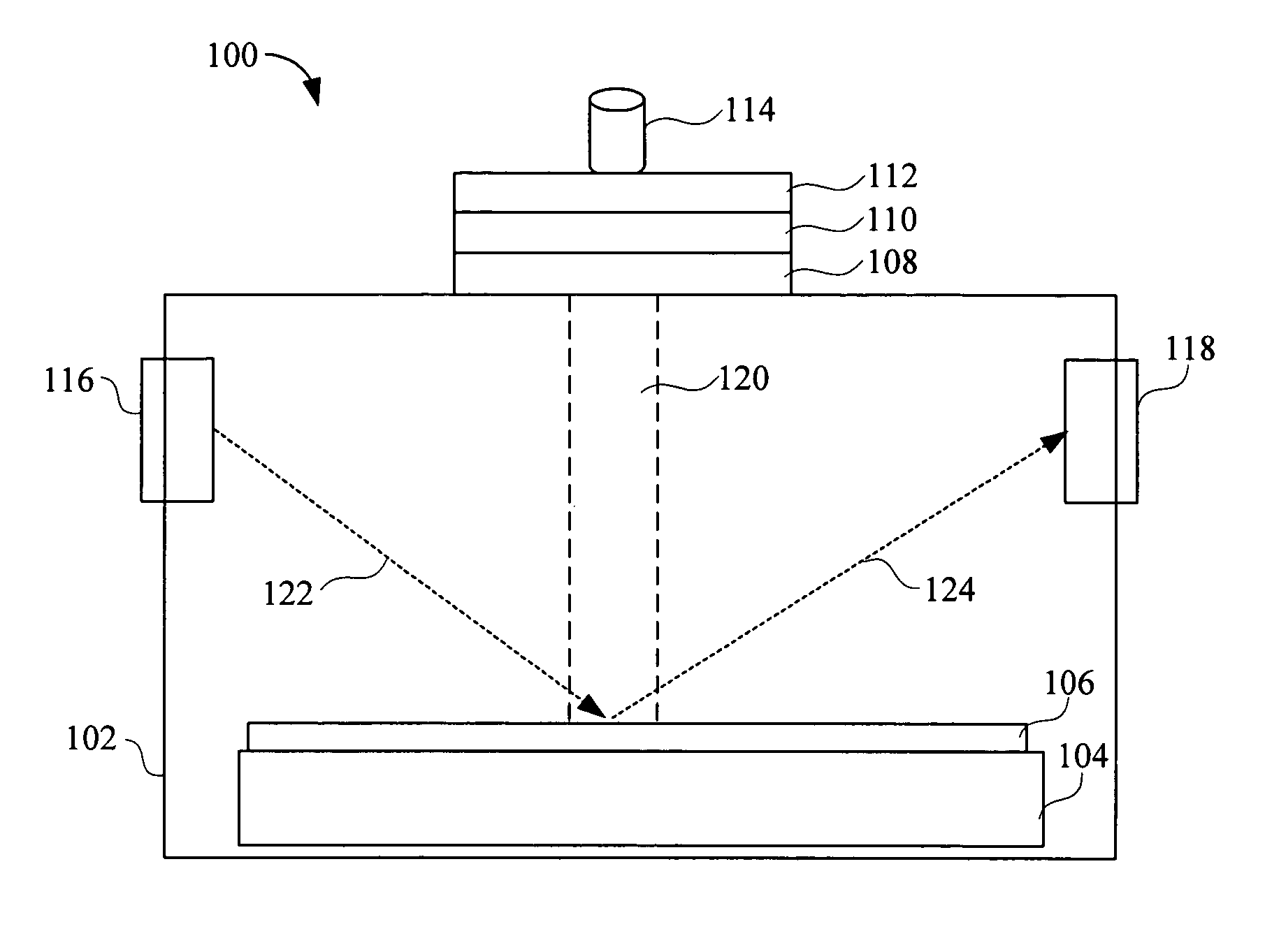
[0033] An invention for determining and selecting which region of a die to use to determine process end point in plasma etch operations is described. In preferred embodiments, methods and systems for the detection and analysis of optical signals using spectral reflectometry include implementing a 2-D CCD detector array to resolve outputs from a plurality of optical signals, and then matching the analyzed signals to model endpoint or exact depth signals to enable essentially absolute etch-to-depth and endpoint calls. In the following description, numerous specific details are set forth in order to provide a thorough understanding of the present invention. It will be understood, however, to one skilled in the art, that the present invention may be practiced without some or all of these specific details. In other instances, well known process operations have not been described in detail in order not to unnecessarily obscure the present invention.
[0034] As an overview, embodiments of t...
PUM
| Property | Measurement | Unit |
|---|---|---|
| diameter | aaaaa | aaaaa |
| diameter | aaaaa | aaaaa |
| spot size | aaaaa | aaaaa |
Abstract
Description
Claims
Application Information