

Package-to-package stacking by using interposer with traces, and or standoffs and solder balls
a technology of interposer and stacking, applied in the field of electronic packaging, can solve the problems of limited use of direct p2p stacking packages, and limited alignment requirements of conventional packaging electronic devices. to achieve the effect of improving the package-to-package stacking assembling process
- Summary
- Abstract
- Description
- Claims
- Application Information
AI Technical Summary
Benefits of technology
Problems solved by technology
Method used
Image

Examples
Embodiment Construction
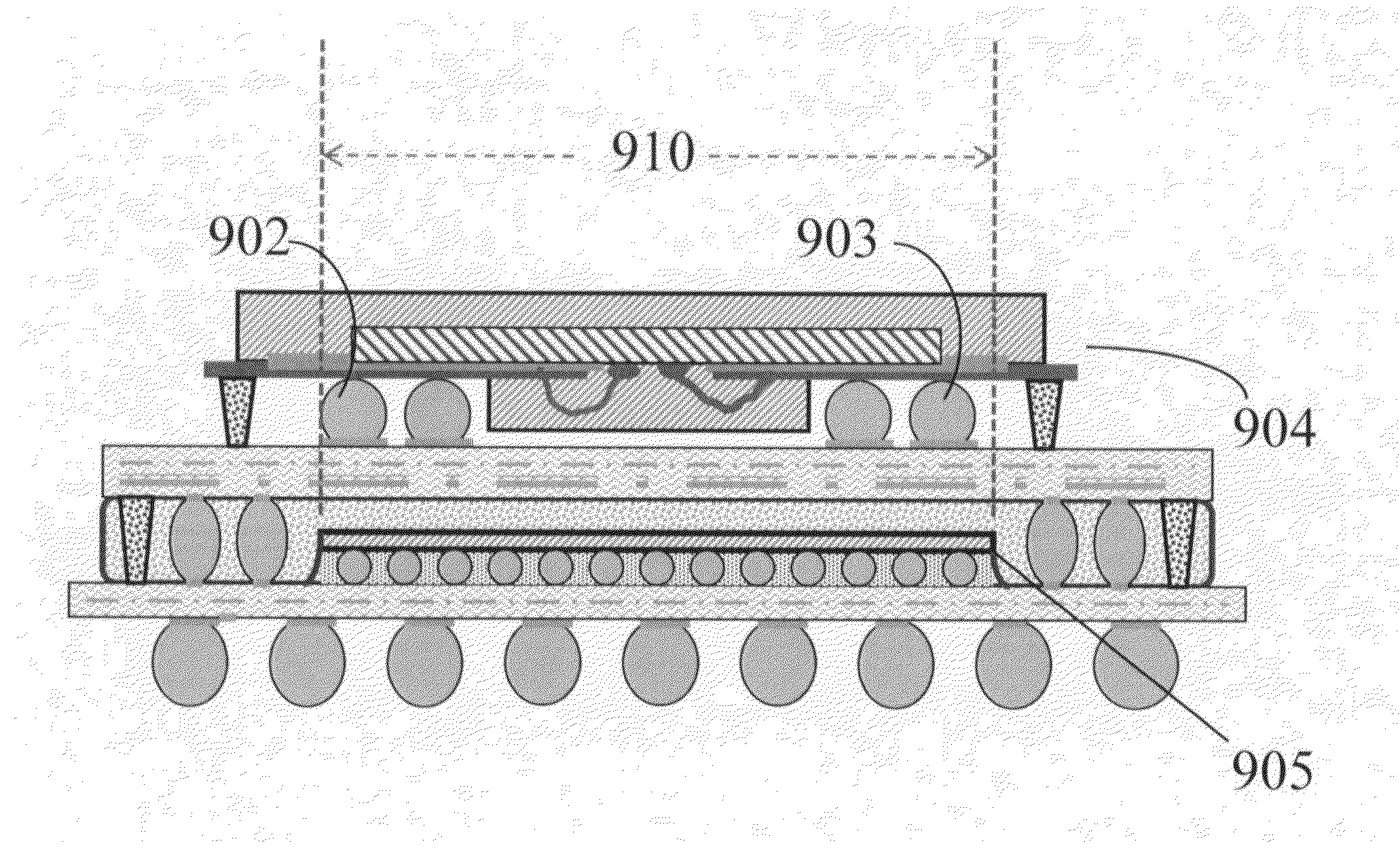
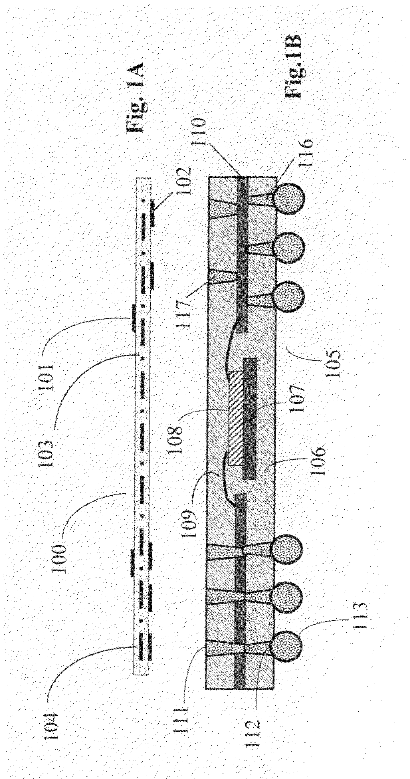
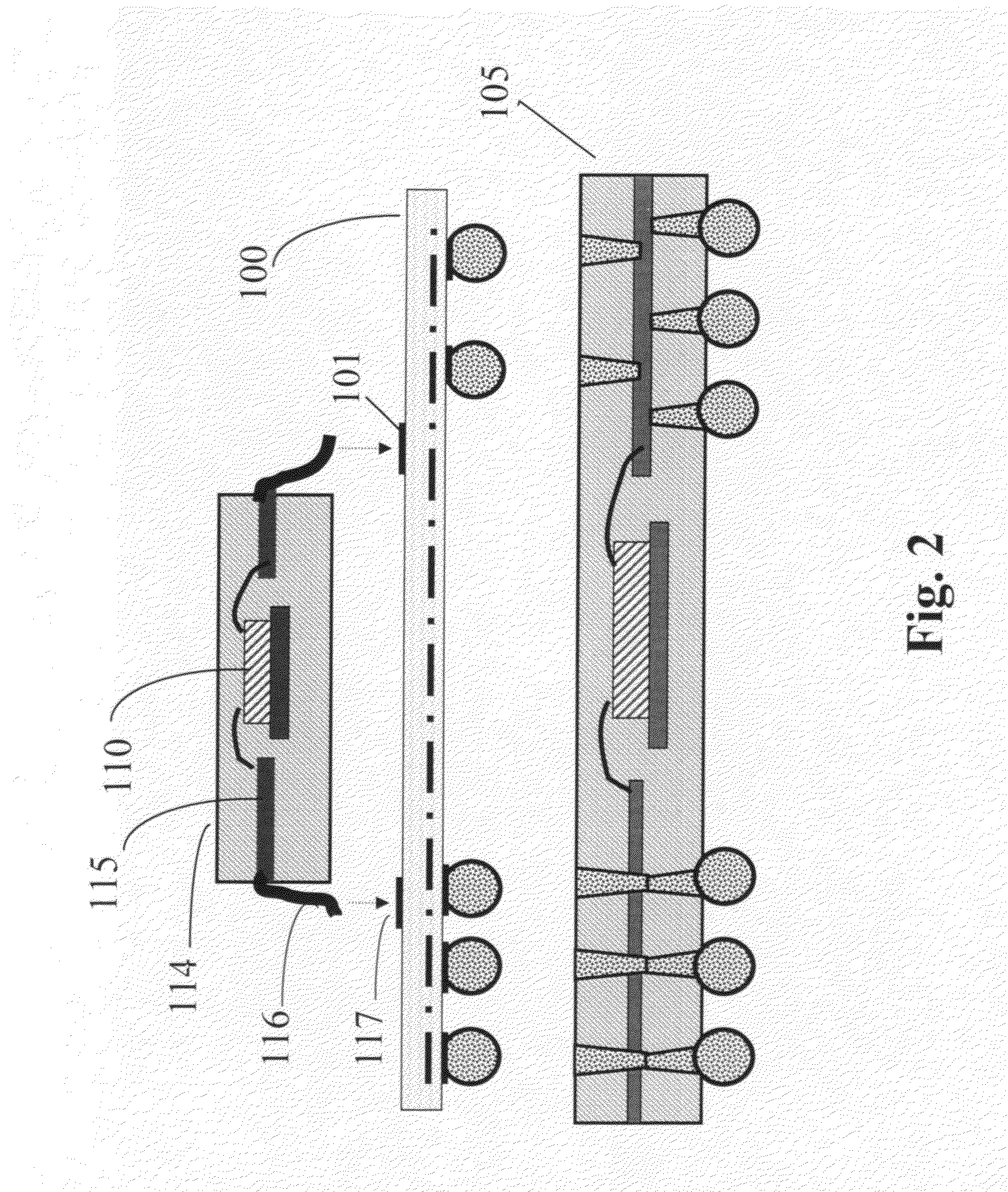
[0030]FIG. 1A is a cross sectional view of a customized printed circuit board (PCB) interposer 100 that is designed to provide interconnecting electrical routing from a top package 114 (FIG. 2) and mounted on top of the interposer, to a bottom package 105 as that shown in FIG. 1B. Additional packaging features and options are further described below. The interposer 100 shown in FIG. 1A has a top surface that includes a top contact pad 101 and the interposer 100 further has a bottom surface that includes bottom contact pads 102. The bottom contact pads 102 are arranged with a layout that matches with the via-holes contact 111 and 117 located on the top side of the bottom package 105 shown in FIG. 1B. The interposer 100 is formed with laminated core layers, 103 that include connecting trace 104 disposed in the intermediate layers of the PCB and connect to the bottom contact pad 102.
[0031]The bottom package 105 shown in FIG. 1B comprises a leadframe package that included a molded lead ...
PUM
 Abstract
Description
Claims
Application Information