Method of formation of nanowires and method of manufacture of associated optical component

a nanowire and optical component technology, applied in the direction of crystal growth process, radiation therapy, photometry, etc., can solve the problems of nanowire centrifugation, high cost and complexity of equipment required for implementing the method, and the use of metals with much higher temperatures, so as to achieve the effect of substantially improving the centrifugation problem

Inactive Publication Date: 2012-01-26
COMMISSARIAT A LENERGIE ATOMIQUE ET AUX ENERGIES ALTERNATIVES
View PDF8 Cites 16 Cited by
  • Summary
  • Abstract
  • Description
  • Claims
  • Application Information

AI Technical Summary

Benefits of technology

[0006]Gold colloids (particles of diameter less than 100 nm) are deposited on the surface of a semiconductor wafer. The substrates are placed in an apparatus, where the colloids are heated to their melting point. Precursor gases are introduced into the apparatus, causing semiconductor saturation in the metal drop. Crystalline growth occurs at the liquid-solid interface by precipitation. The diameter of the nanowires is determined by the size of the drop of metal-semiconductor alloy, which is itself determined by the original size of the gold colloids. Use of gold colloids allows better control of the diameter of the wires than use of a thin metal layer.
[0032]The method of formation of nanowires of the invention uses an optical trap to convey and deposit metal particles (generally nanoshells) on the surface of a semiconductor substrate attached on a solid immersion lens. The metal particles are then used as catalysts for the growth of nanowires by the known methods such as, for example, the VLS method. The metal particles, and consequently the nanowires, are advantageously positioned with an accuracy of the order of some ten nanometres. Advantageously, for the production of an optical component fitted with a solid immersion lens coupled with a nanowire, the solid immersion lens forming part of the optical component participates in the formation of the nanowire. The problem of centring of the nanowire is substantially improved by this means.

Problems solved by technology

However, these metals require the use of much higher temperatures.
There are, however, many disadvantages, namely the cost and complexity of the equipment required for implementing the method (for example the cost of the masks for optical lithography).
The wires produced using this method have uniform diameter and length, but also have several crystallographic faults.
The cost and complexity of the equipment are, however, real disadvantages, as is the situation occupied by the nanowires, which are located in holes.
The advantage of this third method is that satisfactory regularity of the pattern is obtained; the disadvantage lies in the inability to produce random patterns.
The disadvantages are the slow speed of movement of the AFM point, the fact that a single colloid is manipulated at once, and the fact that the method cannot be used if the surface of the silicon substrate has substantial changes of topography.
The disadvantages are that random patterns cannot be produced, and that the nanowires are in holes.
A major disadvantage of such a method is the cost of the mould.
This method of manufacturing an optical component has a major difficulty, namely the centring of the etched twin layer on the lens.
Decentring of the order of magnitude of the diameter of the nanowire (for example few tens to a few hundreds of nanometres) is sufficient, when the optical component has been completed, for it no longer to be possible to couple in the nanowire the light injected in the lens.

Method used


Image

  • Method of formation of nanowires and method of manufacture of associated optical component
  • Method of formation of nanowires and method of manufacture of associated optical component
  • Method of formation of nanowires and method of manufacture of associated optical component

Examples


Embodiment Construction

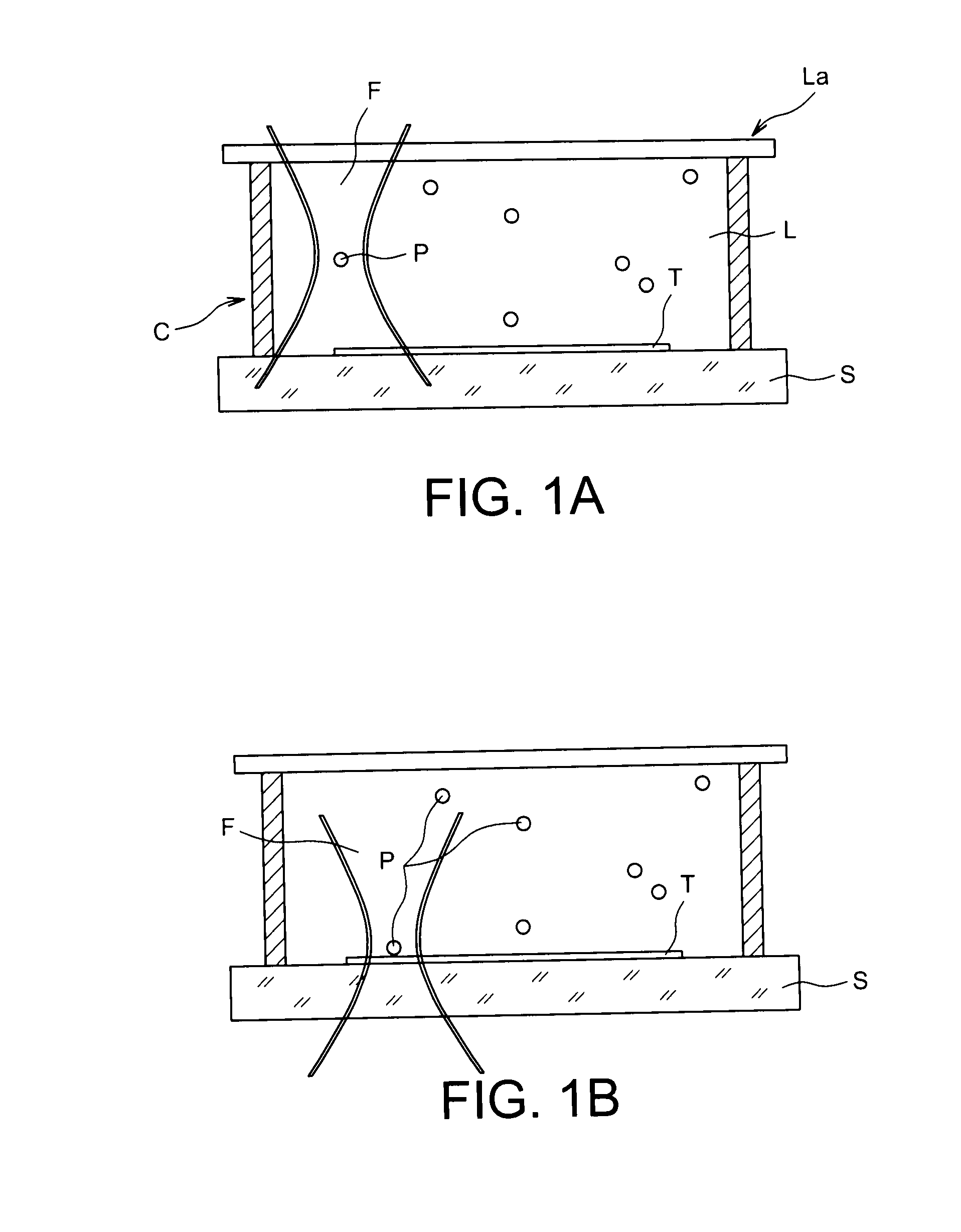
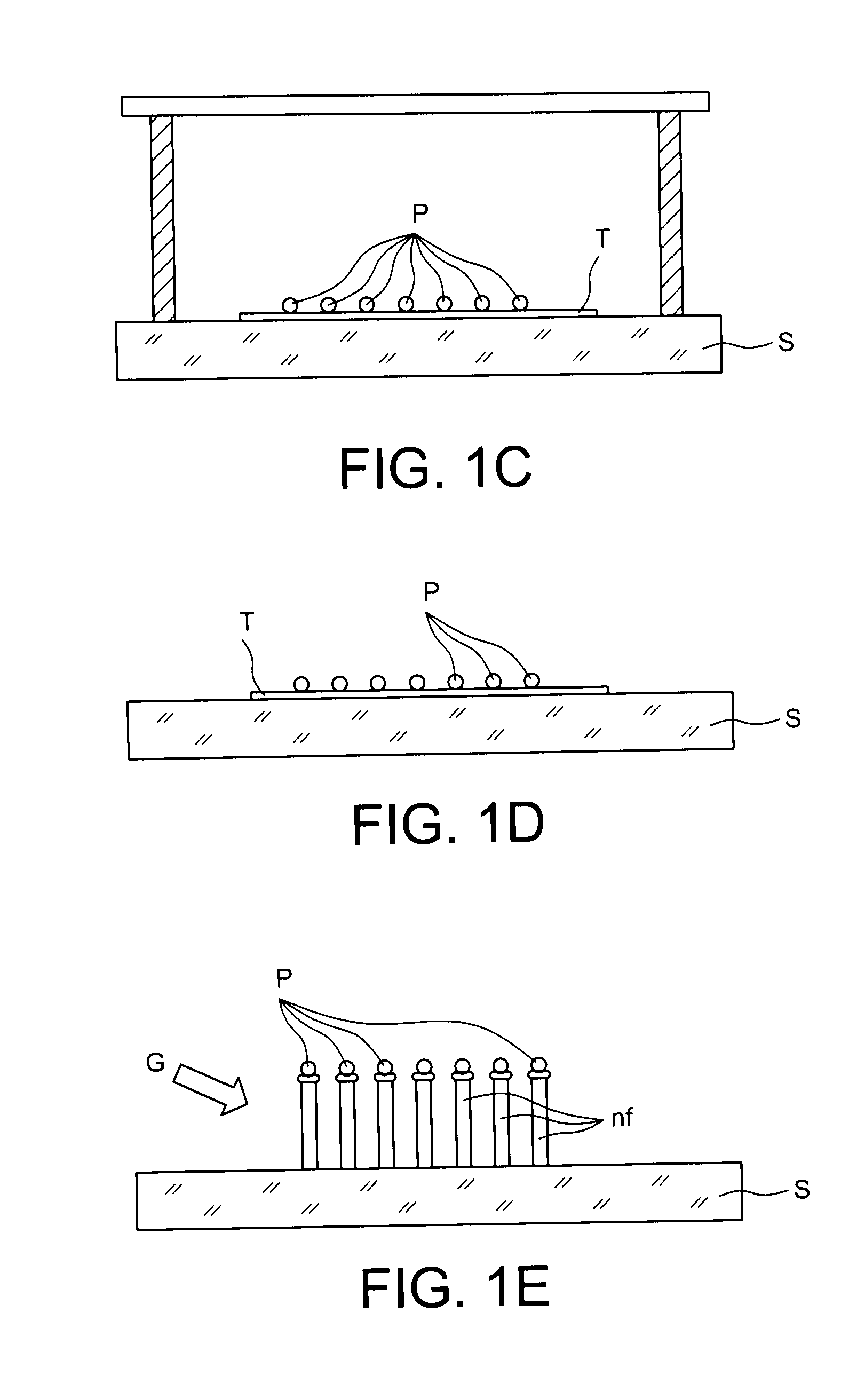
[0047]FIGS. 1A-1F represent successive steps of a method for positioned growth of nanowires on a substrate.

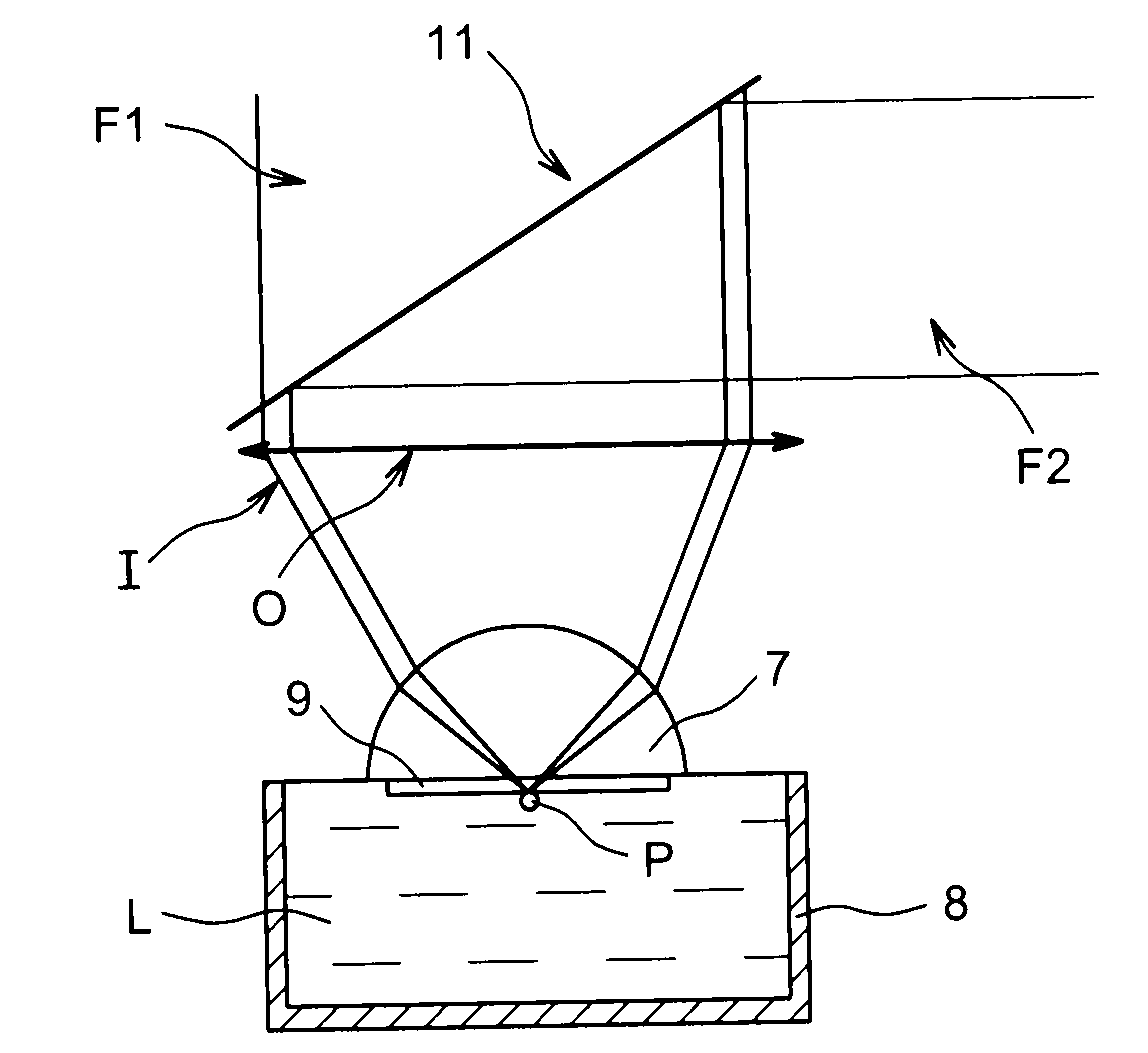
[0048]The optical clip is a light beam waist formed using a microscope objective the numerical aperture of which is greater than 1. The light beam from which the waist is formed is preferentially a laser beam.

[0049]Metal nanoparticles P are placed in a tank C containing a fluid, for example a liquid L. The bottom of the tank C consists of a semiconductor substrate S. An cover glass La constitutes, for example, a lid closing the tank. The face of the semiconductor substrate intended to be in contact with the liquid L has preferentially previously been cleaned by a known method, for example a method of the oxygen plasma treatment type. Also preferentially, a surface treatment T, for example a treatment using poly-L-lysine or treatment by aminosilane, covers the face of the semiconductor substrate which is in contact with the liquid in order to facilitate attachment of the particl...


PUM

PropertyMeasurementUnit
eutectic temperatureaaaaaaaaaa
diameteraaaaaaaaaa
widthaaaaaaaaaa

Abstract

A method of formation of nanowires at a surface of a substrate attached to a solid immersion lens. The method includes formation of a catalyst element at the surface of the substrate and growth of nanowires from the catalyst element formed at the surface of the substrate. The catalyst element is a metal nanoparticle and the formation of the catalyst element at the surface of the substrate deposits the metal nanoparticle using a light beam focused by the solid immersion lens at the surface of the substrate.

Description

TECHNICAL FIELD AND PRIOR ART[0001]The invention concerns a method of formation of nanowires at the surface of a substrate and, more particularly, a method of formation of nanowires at the surface of a substrate attached to the flat face of a solid immersion lens.[0002]The invention also concerns a method of manufacture of an optical component which includes a step of formation of nanowire in accordance with the method of formation of nanowire of the invention.[0003]The invention applies to nanowire manufacturing technologies such as, for example, bottom-up technology. The fields concerned by the invention are those of microelectronics, lighting, photovoltaics, etc.[0004]There are different methods of growing nanowires. Among the best-known is the VLS method (VLS for “Vapour-Liquid-Solid”), which uses a metal catalyst. The metal most commonly used as a catalyst is gold, due to the low eutectic temperature of the gold-silicon blend, which is only 363° C. Gold therefore allows growth ...

Claims


Application Information

Patent Timeline
Patent Type & Authority Applications(United States)
IPC IPC(8): H01L21/02B82Y99/00
CPCC30B29/60C30B11/12
Inventor NEEL, DELPHINEFERRET, PIERREGETIN, STEPHANE
Owner COMMISSARIAT A LENERGIE ATOMIQUE ET AUX ENERGIES ALTERNATIVES
Why Eureka
Try Eureka