Nanoparticle Plasmon Scattering Layer for Photovoltaic Cells

a photovoltaic cell and nanoparticle technology, applied in nanotechnology, coatings, semiconductor devices, etc., can solve the problems of reducing photocurrent, compromising the efficiency of blue photon absorption, and reducing photocurren

Inactive Publication Date: 2012-02-09
NANOSYS INC
View PDF2 Cites 28 Cited by
  • Summary
  • Abstract
  • Description
  • Claims
  • Application Information

AI Technical Summary

Benefits of technology

[0010]Suitably, the compositions further comprise one or more fluorescent nanoparticles. The compositions can comprise a single layer comprising the metal nanoparticles and the fluorescent nanoparticles, or can comprise at least two layers, wherein the colloidal metal nanoparticles and the fluorescent nanoparticles are in separate layers.
[0011]Exemplary the fluorescent nanoparticles for use in the practice of the present invention include, but are not limited to, CdSe, ZnSe, ZnTe and InP nanoparticles. Suitably, the fluorescent nanoparticles comprise a core selected from the group consisting of CdSe, ZnSe, ZnTe and InP, and a shell selected from the group consisting of ZnS and CdS surrounding the core. Suitably, the core is doped with Mn or Cu. In exemplary embodiments, the core is about 1 nm to about 6 nm in size, and the shell is less than about 2 nm in thickness, suitably about 1 Å to about 10 Å in thickness.
[0012]In exemplary embodiments, the transparent substrate comprises glass. In further embodiments, the photovoltaic cell comprises one or more hydrogenated amorphous silicon layers. Suitably the photovoltaic cell comprises one or more hydrogenated amorphous silicon layers, and one or more hydrogenated microcrystalline or hydrogenated nanocrystalline silicon layers.
[0013]Suitably, interfaces between the hydrogenated amorphous silicon layers (including interfaces between the one or more hydrogenated microcrystalline or hydrogenated nanocrystalline silicon layers) are substantially non-textured, and in further embodiments, interfaces between the hydrogenated amorphous silicon layers, and interfaces between the hydrogenated amorphous silicon layers and an electrode of the photovoltaic cell, are substantially non-textured.

Problems solved by technology

However, if the cells are made thick enough to capture most of the red photons, the efficiency of the absorption of blue photons is compromised.
However, this surface roughening also causes more recombination sites to be produced at the layer interfaces and enhances hole electron recombination, reducing the photocurrent, and is also a costly and time-consuming process.

Method used


Image

  • Nanoparticle Plasmon Scattering Layer for Photovoltaic Cells
  • Nanoparticle Plasmon Scattering Layer for Photovoltaic Cells
  • Nanoparticle Plasmon Scattering Layer for Photovoltaic Cells

Examples


Embodiment Construction

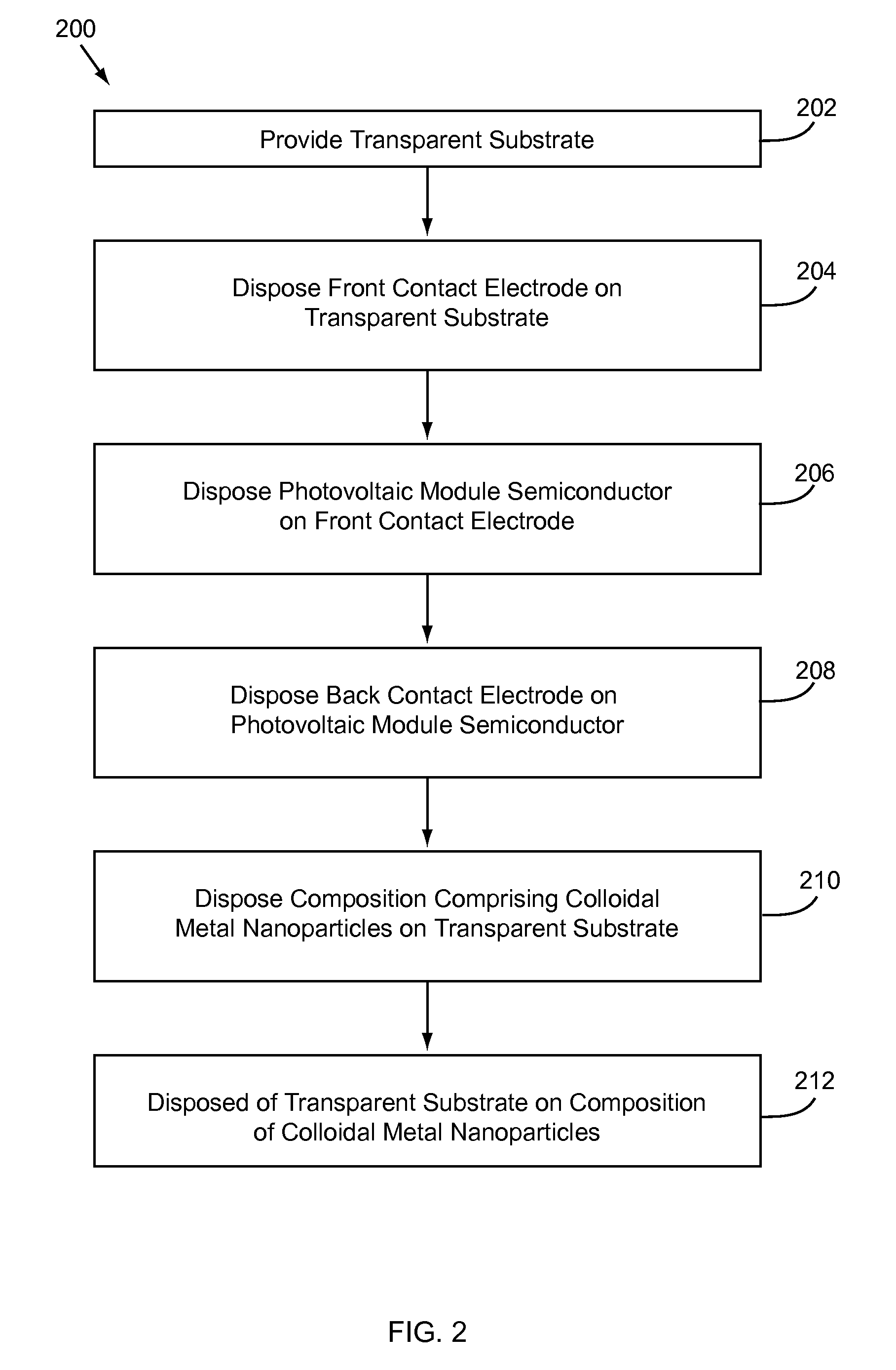
[0024]It should be appreciated that the particular implementations shown and described herein are examples of the invention and are not intended to otherwise limit the scope of the present invention in any way. Indeed, for the sake of brevity, conventional electronics, manufacturing, semiconductor devices, and nanocrystal, nanoparticle, nanowire (NW), nanorod, nanotube, and nanoribbon technologies and other functional aspects of the systems (and components of the individual operating components of the systems) may not be described in detail herein. Further, the techniques are suitable for applications in electrical systems, optical systems, consumer electronics, industrial or military electronics, wireless systems, space applications, or any other application.

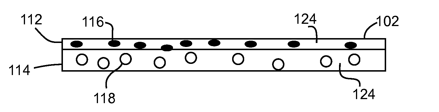
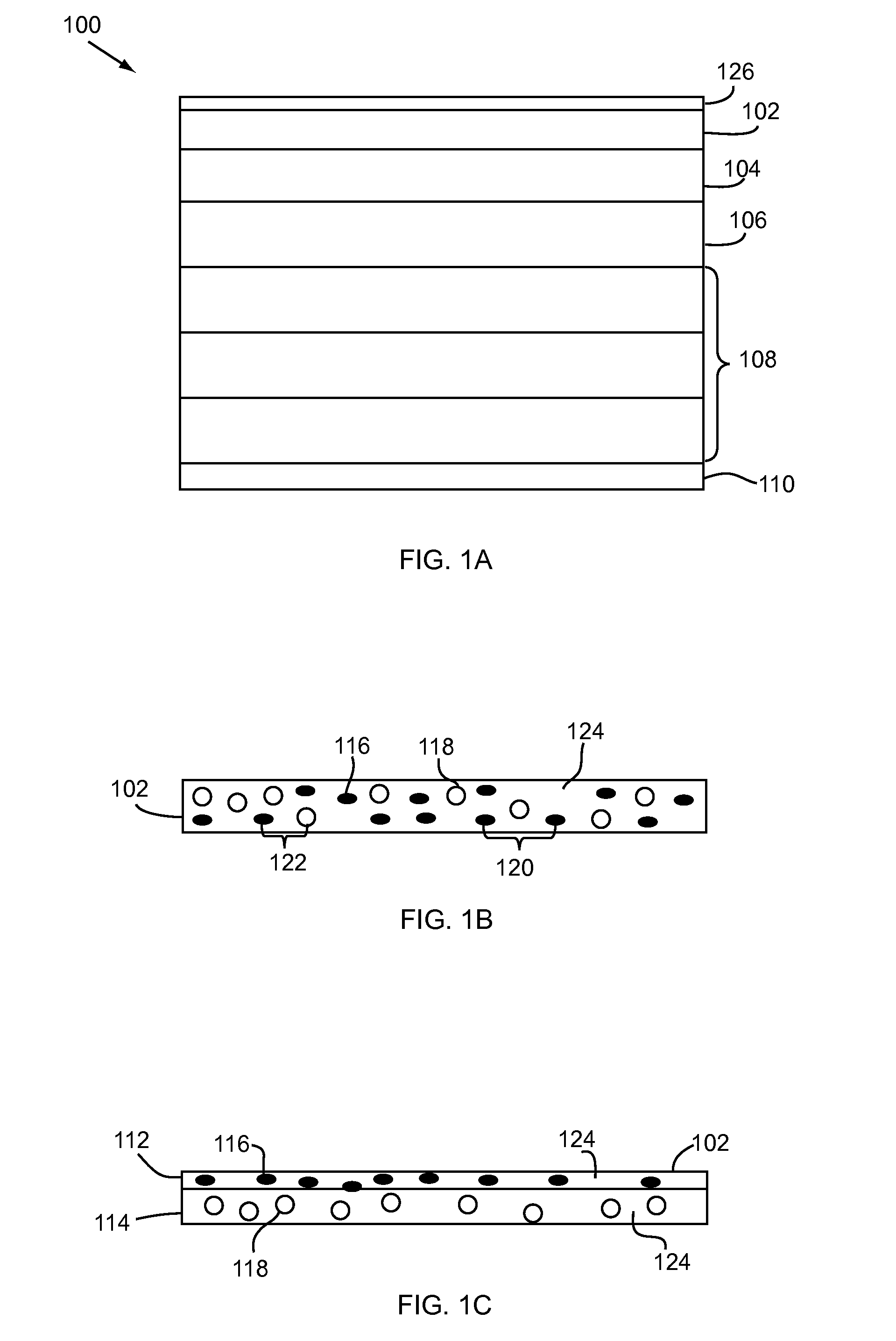
[0025]As used herein, the term “nanoparticle” refers to a particle that has at least one region or characteristic dimension with a dimension of less than about 500 nm, including on the order of less than about 1 nm. The term “n...


PUM

PropertyMeasurementUnit
sizeaaaaaaaaaa
sizeaaaaaaaaaa
sizeaaaaaaaaaa

Abstract

The present invention relates to nanoparticle compositions for use in photovoltaic cells. Nanoparticles are utilized to provide increased scattering and also wavelength shifting to increase the efficiency of the photovoltaic cells. Exemplary nanoparticles include colloidal metal and fluorescent nanoparticles.

Description

BACKGROUND OF THE INVENTION[0001]1. Field of the Invention[0002]The present invention relates to nanoparticle compositions for use in photovoltaic cells. Nanoparticles are utilized to provide increased scattering and also wavelength shifting to increase the efficiency of the photovoltaic cells.[0003]2. Background Art[0004]Photovoltaic cells often utilize active area materials such as silicon as photo-absorbing elements. Typically, such materials absorb more strongly in the blue region of the spectrum than in the red to infrared region. Therefore, layers of the photovoltaic cell are often made thicker to absorb (capture) most of the photons in the red region of the solar spectrum. However, if the cells are made thick enough to capture most of the red photons, the efficiency of the absorption of blue photons is compromised. As a result of these two competing effects a compromise is struck in which some of the blue photons are lost to recombination, and some of the red photons are lost...

Claims


Application Information

Patent Timeline
Patent Type & Authority Applications(United States)
IPC IPC(8): H01L31/0216B05D5/12H01L31/18B82Y99/00
CPCH01L31/02168Y02E10/52H01L31/0384H01L31/055H01L31/02322
Inventor PARCE, J. WALLACECHEN, JIAN
Owner NANOSYS INC
Why Eureka
Try Eureka