Semiconductor heat treatment member having sic film

Inactive Publication Date: 2012-02-16
ASAHI GLASS CO LTD
View PDF4 Cites 0 Cited by
  • Summary
  • Abstract
  • Description
  • Claims
  • Application Information

AI Technical Summary

Benefits of technology

[0041]Heretofore, along with miniaturization of semiconductors, the tolerable deposit thickness of the deposit film becomes thin, and the frequency of cleaning steps has been increased to significantly decrease the throughput of wafer process. However, by employing

Problems solved by technology

By repeating film-deposition steps, the thickness of such a deposit film increases according to the number of film-deposition steps, and when the thickness exceeds a predetermined thickness, formation of cracks in the deposit film or peeling of the deposit film occurs.
Particularly, in a silicon nitride film, since internal stress is formed during the film-deposition, the cracks or peeling occurs even when the film is relatively thin, and the particles tend to be generated.
However, the increase of the frequency of the cleaning step not only increases the cleaning cost but also significantly reduces the throughput of the wafer process, which causes increase of semiconductor production cost.
Particularly, a silicon nitride film generating particles even when the film is relatively thin causes a serious problem.

Method used


Image

  • Semiconductor heat treatment member having sic film
  • Semiconductor heat treatment member having sic film
  • Semiconductor heat treatment member having sic film

Examples


example 1

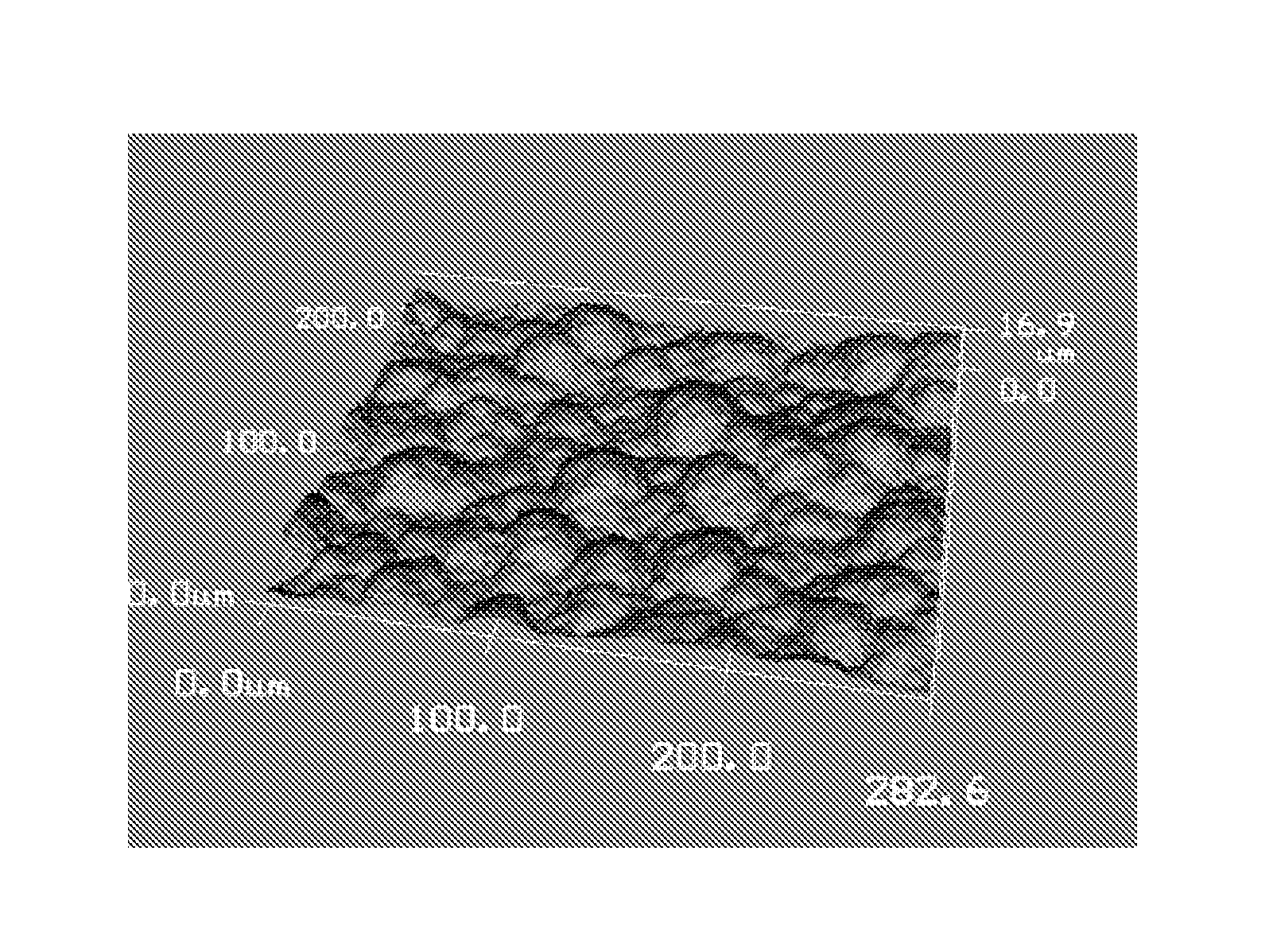
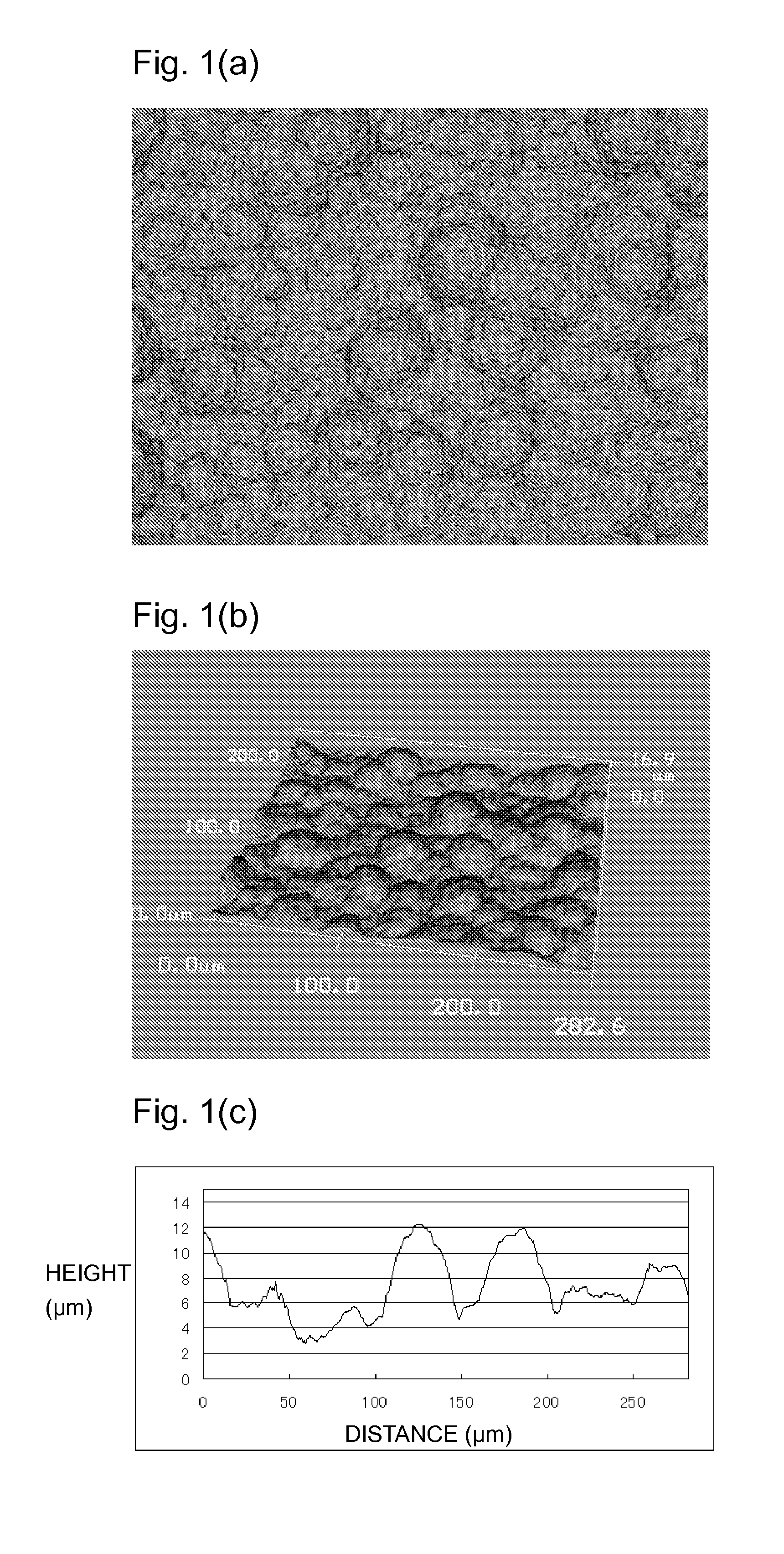
[0092]On SiC substrates, respective CVD-SiC coating films having a thickness of about 60 μm and having various textures were deposited by controlling the film-deposition conditions, to produce substrates, and a silicon nitride film having a thickness of about 6 μm was deposited on each substrate by a LPCVD method. The thickness of the silicon nitride film by each deposition was set to be about 1.5 μm, and after the coating, a forced cooling was carried out with a wind velocity of about 1 m / sec. These operations were repeated four times to form a silicon nitride film having a total thickness of 6 μm. The silicon nitride film was observed by an optical microscope to measure the number of cracks present in the silicon nitride film.

[0093]The texture of the CVD-SiC coating film on the SiC substrate was observed by employing a red laser microscope (manufactured by Keyence Corporation, model VK8710). With a magnification of 500× with an observation length of 282 μm, the texture was measure...

example 2

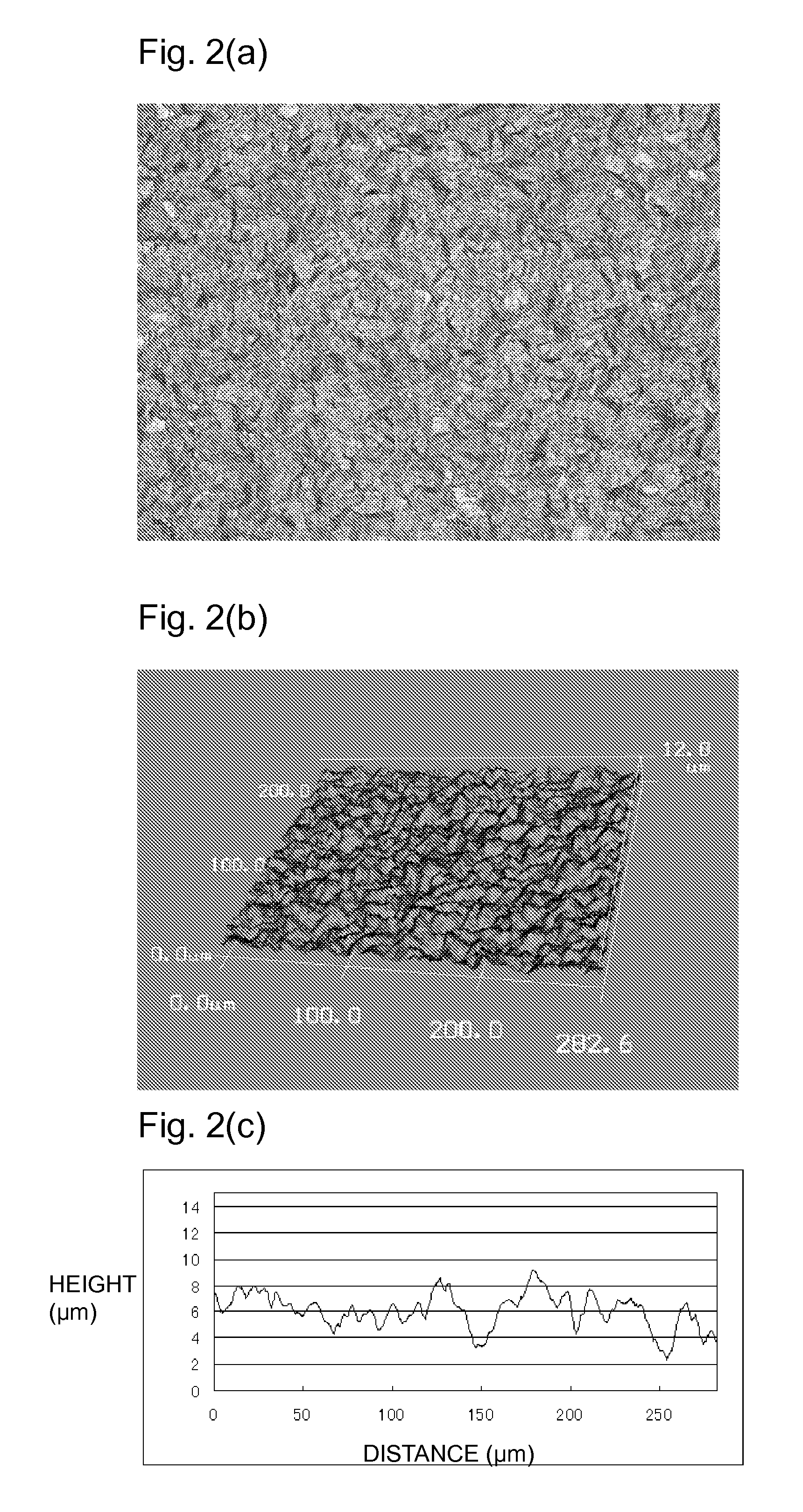
[0097]On SiC substrates, respective CVD-SiC coating films having a thickness of about 60 μm and having textures that I1 was at least 0.9 or I1 was at most 0.9 and I2 was at least 1.6, were deposited by controlling the film-deposition conditions to produce substrates, and on each substrate, a silicon nitride film having a thickness of about 6 μm was deposited by a LPCVD method. The thickness of the silicon nitride film by each deposition was set to be about 1.5 μm, and after the coating, a forced cooling with a wind velocity of about 1 m / sec was carried out, and these operations were repeated four times to form a silicon nitride film having a total thickness of about 6 μm. The silicon nitride film was observed by an optical microscope to measure the number of cracks present in the silicon nitride film so as to classify them into cracks due to peeling of the silicon nitride film and cracks due to brittle fracture by internal stress.

[0098]The texture of the CVD-SiC coating film on the ...


PUM

PropertyMeasurementUnit
Lengthaaaaaaaaaa
Lengthaaaaaaaaaa

Abstract

A semiconductor heat treatment member having a CVD-SiC film, which can reduce the frequency of cleaning steps and significantly improves the throughput of wafer process, is provided.A semiconductor heat treatment member is provided, which has a characteristic that when a Fourier amplitude spectrum of a cross-sectional profile of the CVD-SiC film deposited on the semiconductor heat treatment member obtained by observing the CVD-SiC film by a laser microscope with a magnification of from 400 to 600×, is integrated in ranges of 0.01≦ω≦0.02 and 0.05≦ω≦0.2, to obtain integral values of I1 and I2, respectively, then, I1 is at least 0.9 and 12 is at least 1.6.

Description

TECHNICAL FIELD[0001]The present invention relates to a semiconductor heat treatment member having a SiC film to be used for a low pressure chemical vapor deposition (hereinafter referred to as LPCVD) step in a semiconductor manufacturing process.BACKGROUND ART[0002]A polysilicon film or a silicon nitride film to be deposited on a silicon wafer in a LPCVD step in a semiconductor manufacturing process is not only deposited on the silicon wafer but also deposited on a wafer-supporting jig or on a furnace core tube of a reactor furnace to form the same type of film (hereinafter referred to as deposit film).[0003]By repeating film-deposition steps, the thickness of such a deposit film increases according to the number of film-deposition steps, and when the thickness exceeds a predetermined thickness, formation of cracks in the deposit film or peeling of the deposit film occurs. Accordingly, particles of polysilicon or silicon nitride are generated to form defects of a silicon wafer. Par...

Claims


Application Information

Patent Timeline
IPC IPC(8): G01B11/24B32B3/00
CPCC23C16/325Y10T428/24355C23C16/4404
Inventor KAWAGUCHI, MASANORIKAMISUKI, YOICHIFUKASAWA, YASUJI
Owner ASAHI GLASS CO LTD
Why Eureka
Try Eureka