Power Supply Circuit and Power Conversion Device

a power supply circuit and power conversion technology, applied in the direction of electric variable regulation, process and machine control, instruments, etc., can solve the problems of deterioration of energy efficiency damage to switching devices, etc., and achieve the effect of suppressing the decrease of output voltag

Active Publication Date: 2012-03-01
HITACHI ASTEMO LTD
View PDF3 Cites 21 Cited by
  • Summary
  • Abstract
  • Description
  • Claims
  • Application Information

AI Technical Summary

Benefits of technology

[0010]It is possible to provide a power conversion device which can suppress a decrease of the output voltage to the gate even if the carrier frequency increases.

Problems solved by technology

In this case, there is a problem that the switching device may be damaged when the voltage is beyond its rated voltage.
On the other hand, when the switching speed is slow, surge hardly occurs, but the switching loss of the switching device is large to cause deterioration of the energy efficiency.
In addition, when the switching speed is slow, the junction temperature is apt to increase so that the switching device may be damaged when the temperature is beyond its rated temperature.
In a background-art power supply circuit, with increase in the carrier frequency (switching frequency) of a gate drive circuit, a current with which the capacity in the gate of a switching device is charged / discharged increases to increase power consumption in the gate.
Even if the power supplied to the gate drive circuit is constant, the power consumption of the gate drive circuit increases.
Thus, there arises a problem that the energy efficiency deteriorates due to the increase in switching loss.

Method used


Image

  • Power Supply Circuit and Power Conversion Device
  • Power Supply Circuit and Power Conversion Device
  • Power Supply Circuit and Power Conversion Device

Examples


first embodiment

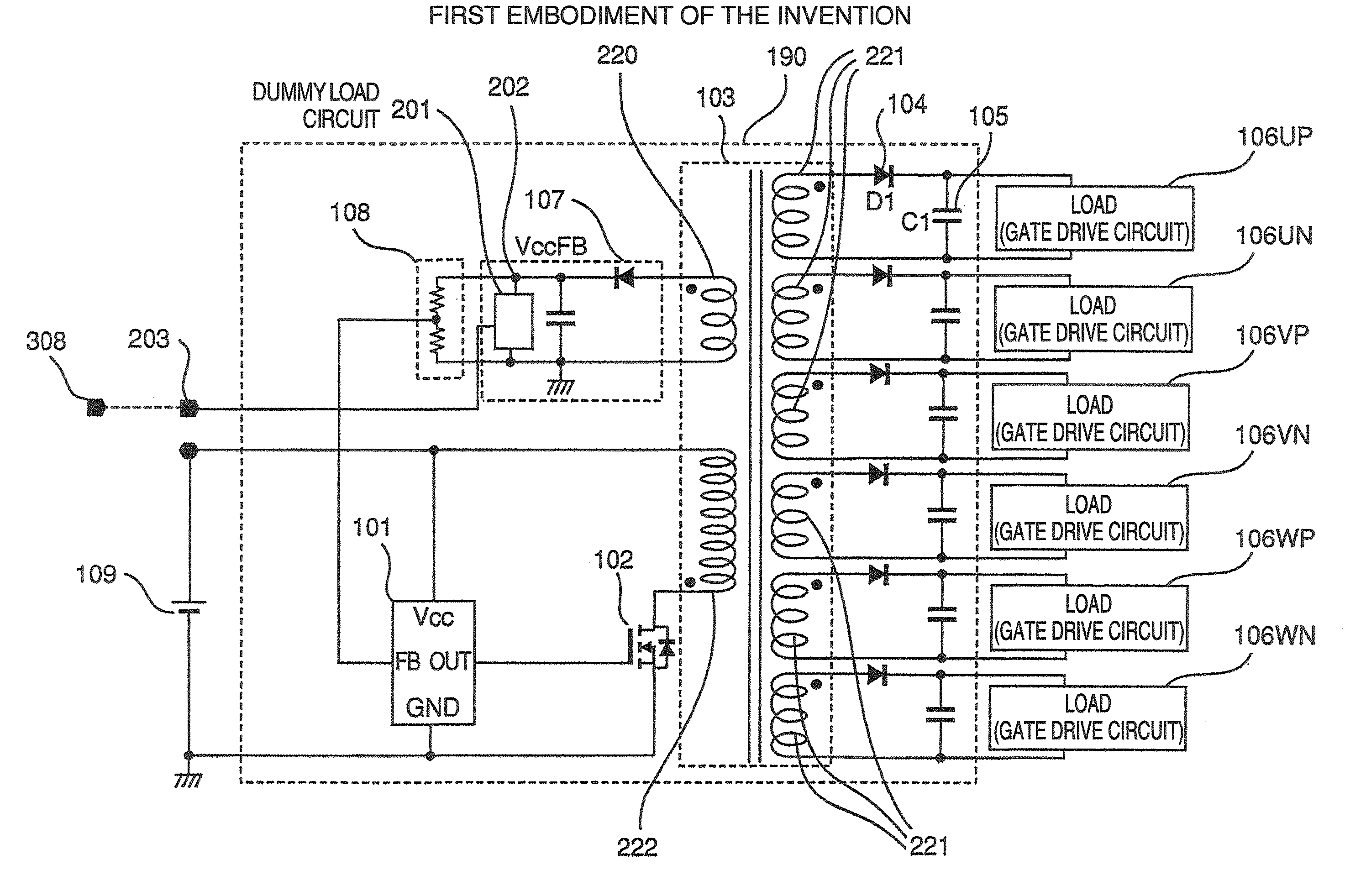
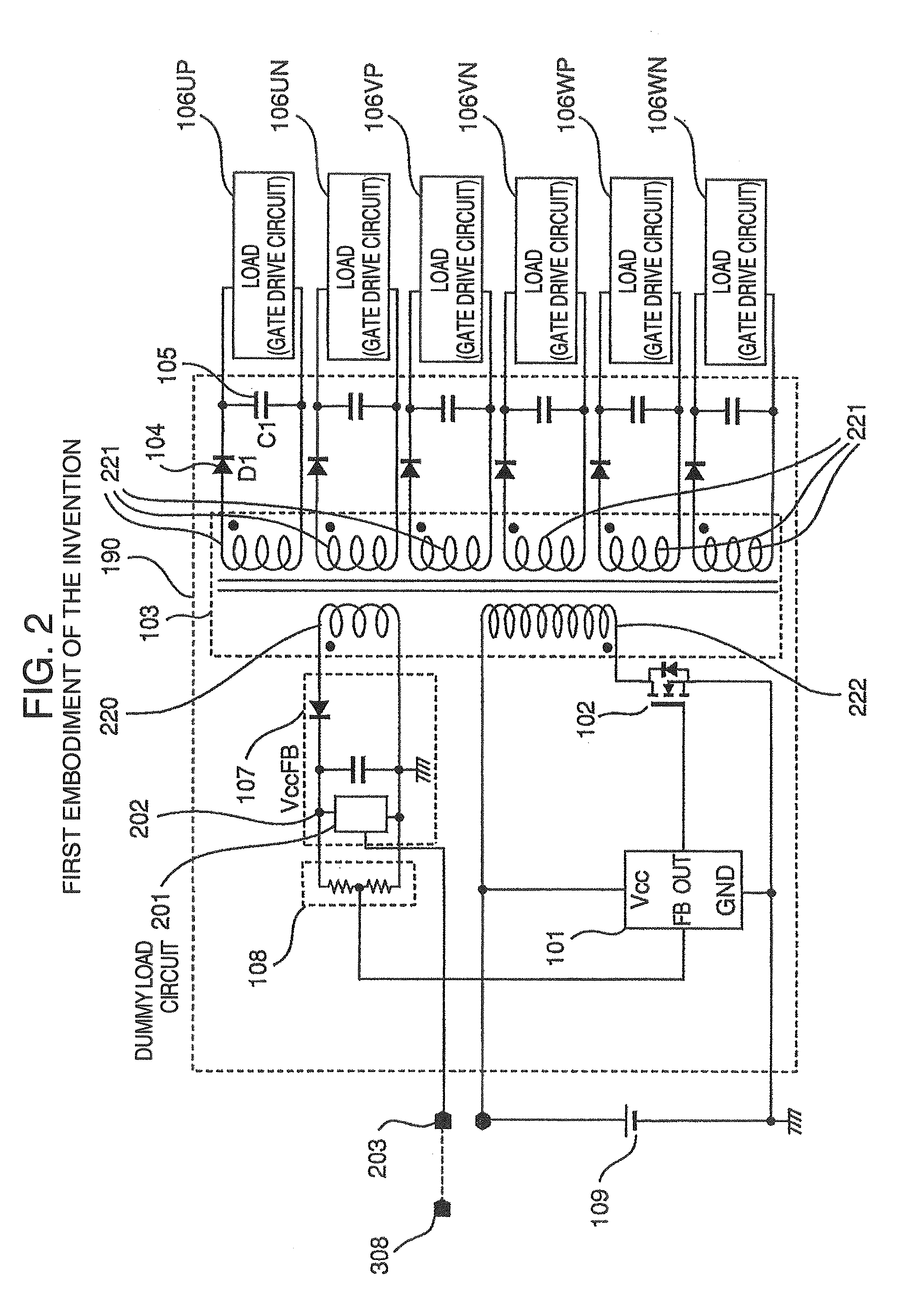
[0026]A first embodiment of the invention will be described with reference to FIG. 2. FIG. 2 represents a power supply circuit for gate drive circuits. The power supply circuit is a flyback type circuit. The power supply circuit has a transformer 103 for insulating outputs. The transformer 103 has one primary coil 222 and seven secondary coils 220 and 221. One of the secondary coils is a dummy coil 220 for feeding back a power supply voltage, and the other six 221 provide power to gate drive circuits 106. A power supply control IC 101 and a transformer driving MOSFET 102 are located on the primary side of the transformer. The primary coil is connected to a battery 109 outside an inverter through a motor control board. The power supply control IC 101 outputs a PWM signal to the gate of the MOSFET 102 so as to switch a primary current of the transformer 103. On that occasion, the primary current of the transformer 103 can be changed in accordance with the duty ratio of the PWM signal ...

second embodiment

Power Supply Circuit

[0042]A second embodiment of the invention will be described with reference to FIG. 8. This power supply circuit 190 has almost the same configuration as the power supply circuit described in the first embodiment. In the first embodiment, power is also supplied to the dummy load circuit so that the power is also consumed in the dummy load circuit. However, since it works out as long as the dummy load circuit can output a feedback output voltage high enough to prevent the output voltage drop of each gate drive circuit 106, it is therefore desirable that the power consumption in the dummy load circuit is suppressed. To this end, this embodiment differs from the first embodiment as follows. That is, the number of turns of a feedback coil 804 of a transformer 803 is reduced to 1 / 3 of the number of turns of any other secondary coil so as to make the voltage division ratio of a voltage divider circuit 805 three times as high as its original one. That is, the output vol...

third embodiment

Power Supply Circuit

[0048]A third embodiment of the invention will be described with reference to FIG. 10. A power supply circuit in this embodiment is substantially the same as the power supply circuit described in the first embodiment. In the first and second embodiments, a gate signal to be outputted to one upper arm or one lower arm is supplied to the dummy load circuit. However, when the control system of the inverter 301 is changed to a two-phase modulation system, there is a fear that feedback cannot be performed due to use of a signal of one phase which is not operative. Accordingly, in the third embodiment, three signal terminals 1004, 1005 and 1006 connected to the motor control board 302 are provided between an output node 1002 of a feedback output circuit 1003 and the ground. Thus, signals based on gate signal information, for example, carrier frequency information can be outputted directly to a dummy load circuit 1001 so as to improve the reliability of control.

[0049]As...


PUM


Abstract

A power conversion device includes an inverter circuit converting DC power into AC power and including switching devices constituting upper and lower arms, a control circuit controlling the switching devices, a drive circuit driving the switching devices by a signal from the control circuit, and an insulated power supply circuit supplying power to the drive circuit. The control circuit controls a power supply voltage to be outputted from the power supply circuit to the drive circuit. The drive circuit drives the switching devices and based on a carrier frequency and the power supply voltage. The power supply circuit includes a feedback output circuit through which the voltage outputted to the drive circuit is outputted to a power supply control IC. The feedback output circuit includes a dummy load circuit which controls the voltage to be outputted to the power supply control IC based on a change of the carrier frequency.

Description

BACKGROUND OF THE INVENTION[0001]The present invention relates to a power supply circuit and a power conversion device for a hybrid car or an electric car.[0002]With increase in the switching speed of a switching device formed as a constituent member of an inverter, the switching loss is reduced, but surge is apt to occur in the collector-emitter voltage of the switching device. In this case, there is a problem that the switching device may be damaged when the voltage is beyond its rated voltage. On the other hand, when the switching speed is slow, surge hardly occurs, but the switching loss of the switching device is large to cause deterioration of the energy efficiency. In addition, when the switching speed is slow, the junction temperature is apt to increase so that the switching device may be damaged when the temperature is beyond its rated temperature.[0003]A gate drive circuit needs to be designed to optimize these trade-offs. It is desirable that a gate voltage does not fluct...

Claims


Application Information

Patent Timeline
Patent Type & Authority Applications(United States)
IPC IPC(8): H02M3/335
CPCH02M1/08H02M2001/0006H02M7/5387H02M3/156H02M3/335H03K17/04123H02M1/0006H02M1/0025
Inventor FUNABA, SEIJINOTO, YASUOTSUJI, MASASHIGE
Owner HITACHI ASTEMO LTD
Why Eureka
Try Eureka