

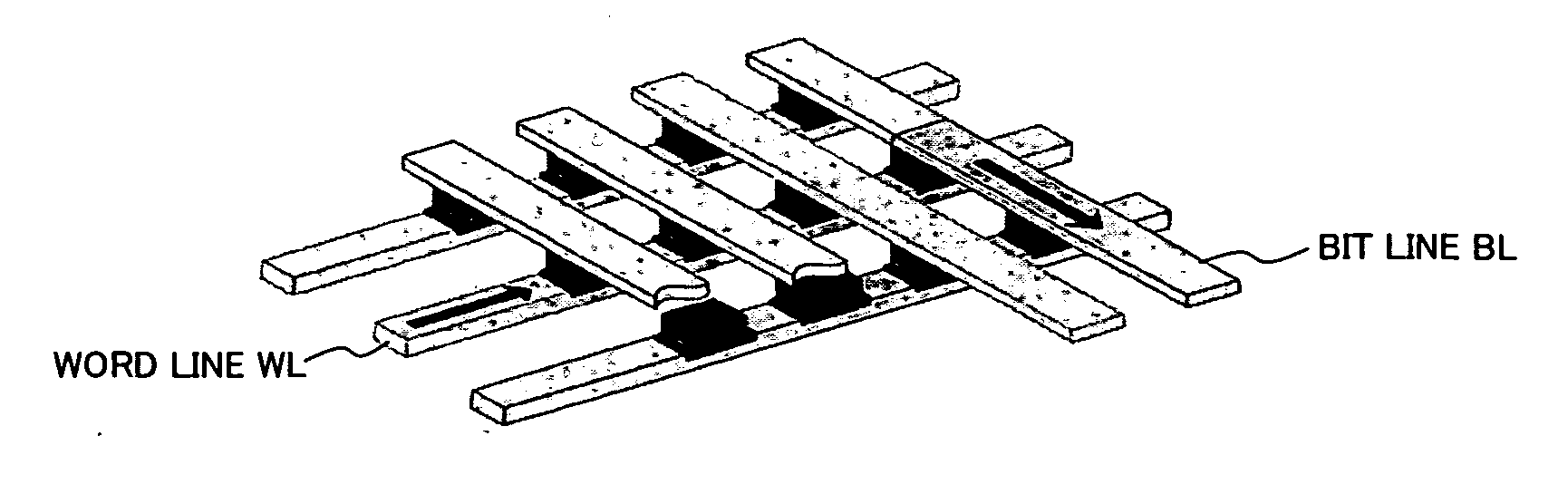
Magnetic tunnel junction device and method of manufacturing the same
- Summary
- Abstract
- Description
- Claims
- Application Information
AI Technical Summary
Benefits of technology
Problems solved by technology
Method used
Image

Examples
first embodiment
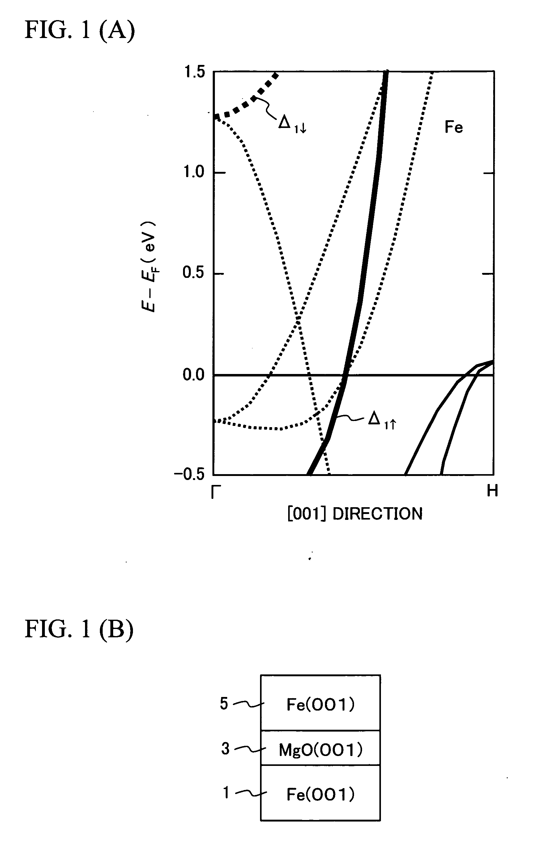
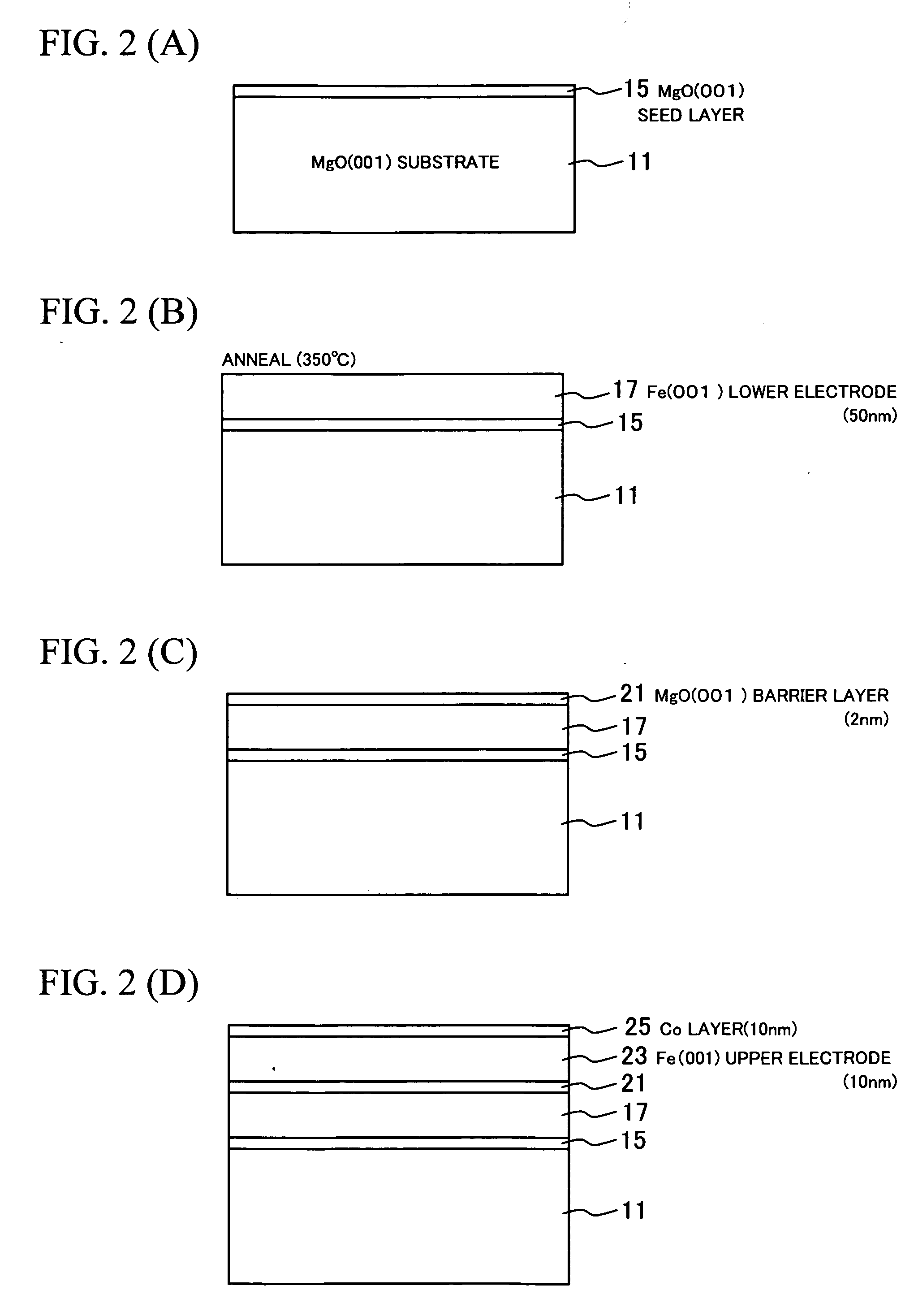
[0033] In the following, a MTJ device according to the invention and a method of manufacturing the same will be described with reference to the drawings. FIGS. 2(A) to 2(D) schematically show the method of manufacturing the MTJ device having the Fe (001) / MgO(001) / Fe(001) structure according to the embodiment (to be hereafter referred to as a “Fe(001) / MgO(001) / Fe(001) MTJ device”). Fe(001) refers to a ferromagnetic material with the BCC structure. First, a single-crystal MgO(001) substrate 11 was prepared. In order to improve the morphology of the surface of the single-crystal MgO(001) substrate 11, a MgO(001) seed layer 15 was grown by the molecular beam epitaxy (MBE) method. This was subsequently followed by the growth of an epitaxial Fe(001) lower electrode (first electrode) 17 with the thickness of 50 nm on the MgO(001) seed layer 15 at room temperature, as shown in FIG. 1(B), and then annealing was performed at 350° C. under ultrahigh vacuum (2×10⁻⁸ Pa). Electron-beam evaporatio...
second embodiment
[0043] Hereafter, a MTJ device according to the invention and a method of manufacturing the same will be described. In the method of manufacturing a Fe(00l) / MgO(001) / Fe(001) MTJ device according to the present embodiment, MgO(001) is initially deposited in a poly-crystalline or amorphous state by sputtering or the like, and then an annealing process is performed such that a poly-crystal in which the (001) crystal plane is preferentially oriented or a single-crystal is obtained. The sputtering conditions were such that, for example, the temperature was room temperature (293K), a 2-inch φMgO was used as a target, and sputtering was conducted in an Ar atmosphere. The acceleration power was 200 W and the growth rate was 0.008 nm / s. Because MgO that is deposited under these conditions is in an amorphous state, a crystallized MgO was obtained by increasing the temperature to 300° C. from room temperature and maintaining that temperature for a certain duration of time.
[0044] Oxygen vacancy...
PUM
 Abstract
Description
Claims
Application Information