Semiconductor device and method for driving the same

a semiconductor and semiconductor technology, applied in pulse generators, pulse techniques, instruments, etc., can solve the problems of easy dielectric breakdown, and achieve the effect of alleviating the concentration of an electric field

Active Publication Date: 2012-03-08
SEMICON ENERGY LAB CO LTD
View PDF4 Cites 6 Cited by
  • Summary
  • Abstract
  • Description
  • Claims
  • Application Information

AI Technical Summary

Benefits of technology

[0014]In the semiconductor device that is one embodiment of the present invention, the concentration of an electric-field can be alleviated.
[0015]By a method for driving the semiconductor device that is one embodiment of the present invention, the concentration of an electric-field can be alleviated.

Problems solved by technology

Therefore, when the drain voltage is increased, an electric field is concentrated in a certain portion, whereby dielectric breakdown easily occurs in a gate insulating film.

Method used


Image

  • Semiconductor device and method for driving the same
  • Semiconductor device and method for driving the same
  • Semiconductor device and method for driving the same

Examples


embodiment 1

[0034]In this embodiment, a semiconductor device that is one embodiment of the present invention will be described.

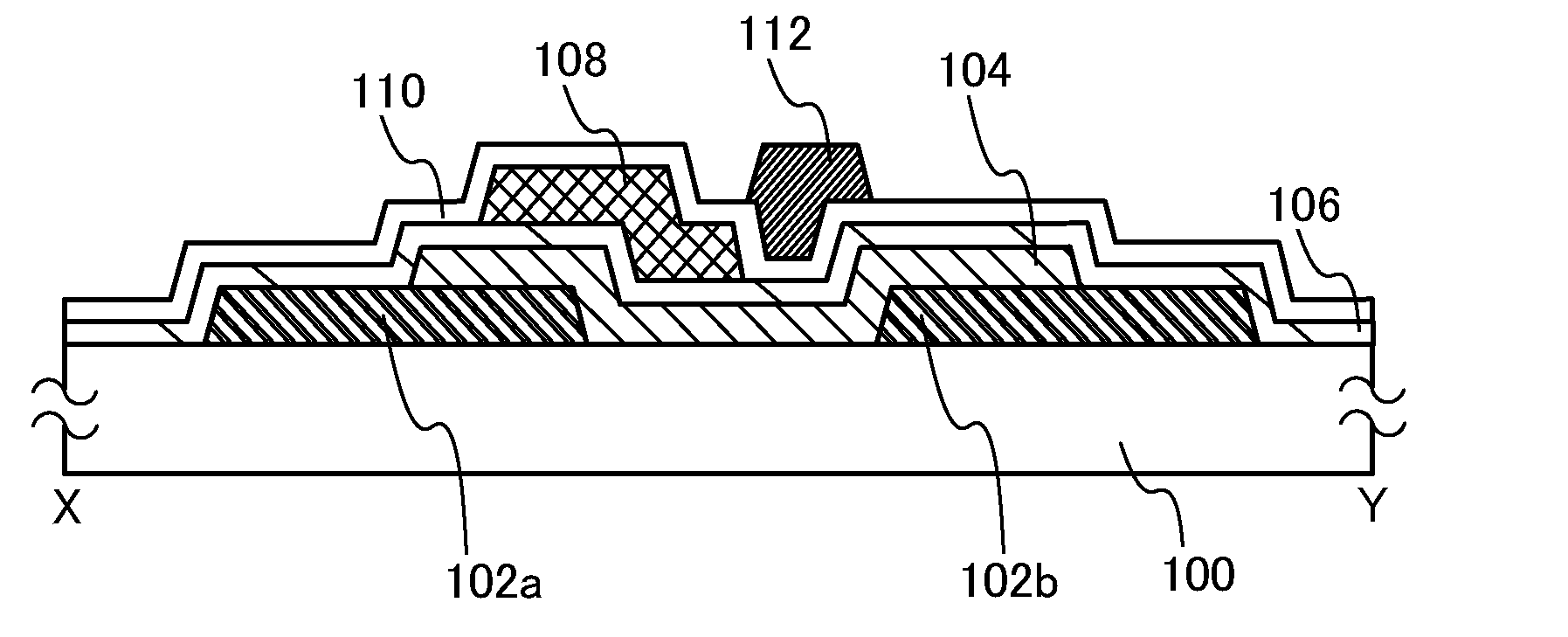
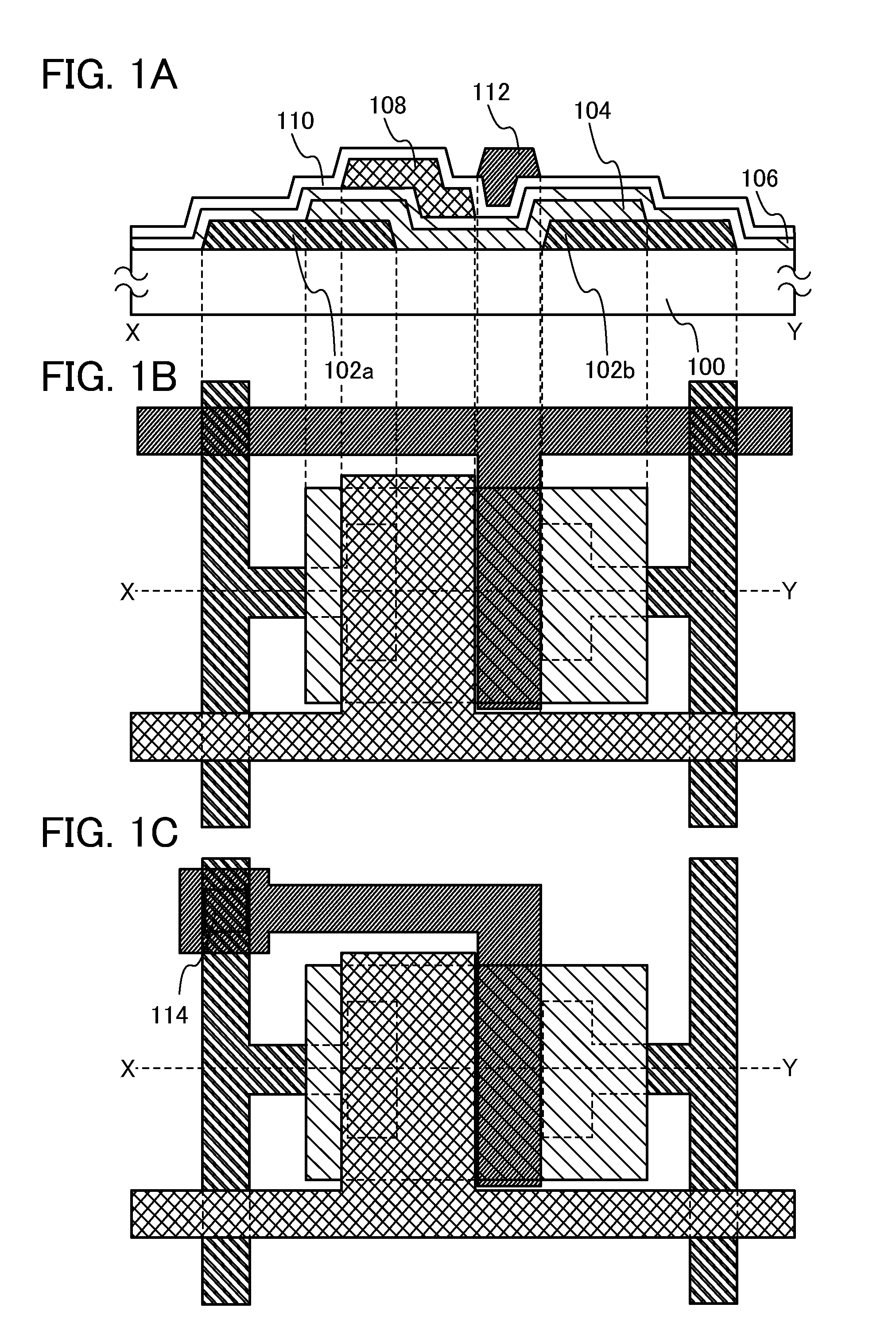
[0035]FIGS. 1A to 1C illustrate a semiconductor device that is one embodiment of the present invention. FIG. 1A is a cross-sectional view of the semiconductor device that is one embodiment of the present invention. FIGS. 1B and 1C are examples of a top view of the semiconductor device that is one embodiment of the present invention. Note that FIG. 1A is a cross-sectional view taken along line X-Y illustrated in FIGS. 1B and 1C.

[0036]The semiconductor device illustrated in FIG. 1A includes a source electrode 102a and a drain electrode 102b provided to be apart from each other over a substrate 100, a semiconductor layer 104 provided between and in contact with the source electrode 102a and the drain electrode 102b, a first insulating layer 106 provided to cover at least the semiconductor layer 104, a gate electrode 108 provided over the first insulating layer 106 to overl...

embodiment 2

[0092]A semiconductor device that is one embodiment of the present invention is not limited to the structure described in Embodiment 1. In this embodiment, a semiconductor device that is one embodiment of the present invention and is different from that of Embodiment 1 will be described.

[0093]FIGS. 12A to 12C illustrate a semiconductor device of this embodiment. FIG. 12A is a cross-sectional view of the semiconductor device that is one embodiment of the present invention. FIG. 12B is an example of a top view of the semiconductor device of this embodiment. FIG. 12C is another example of a top view of the semiconductor device of this embodiment. Note that FIG. 12A is a cross-sectional view taken along line X-Y of in FIG. 12B and FIG. 12C.

[0094]The semiconductor device illustrated in FIGS. 12A and 12B includes a gate electrode 202a and an electric-field control electrode 202b provided over a substrate 200 to be apart from each other, a first insulating layer 204 provided to cover the g...

embodiment 3

[0096]A semiconductor device that is one embodiment of the present invention is not limited to the structures described in Embodiment 1 and Embodiment 2. In this embodiment, a semiconductor device that is one embodiment of the present invention and is different from those in Embodiment 1 and Embodiment 2 will be described.

[0097]FIGS. 13A to 13C illustrate the semiconductor device of this embodiment. FIG. 13A is a cross-sectional view of the semiconductor device that is one embodiment of the present invention. FIG. 13B is an example of a top view of the semiconductor device of this embodiment. FIG. 13C is another example of a top view of the semiconductor device of this embodiment. Note that FIG. 13A is a cross-sectional view taken along line X-Y illustrated in FIGS. 13B and 13C.

[0098]The semiconductor device illustrated in FIGS. 13A and 13B includes a gate electrode 302a and a drain electrode 302b provided over a substrate 300 to be apart from each other, a first insulating layer 30...


PUM


Abstract

An object is to alleviate the concentration of an electric field in a semiconductor device. A gate electrode and a drain electrode are provided not to overlap with each other, and an electric-field control electrode is provided between the gate electrode and the drain electrode over a top surface. Insulating layers are provided between the gate electrode and a semiconductor layer and between the electric-field control electrode and the semiconductor layer, and the insulating layer provided between the electric-field control electrode and the semiconductor layer has a larger thickness than the insulating layer provided between the gate electrode and the semiconductor layer. Further, when the semiconductor device is driven, the potential of the electric-field control electrode may be higher than or equal to a source potential and lower than a gate potential, and for example, connection between the electric-field control electrode and the source potential enables such a structure.

Description

BACKGROUND OF THE INVENTION[0001]1. Field of the Invention[0002]The present invention relates to a semiconductor device and a method for driving the semiconductor device. Note that in this specification, the semiconductor device means a semiconductor element itself or a device including a semiconductor element. As such a semiconductor element, for example, a thin film transistor can be given. Therefore, the semiconductor device includes a liquid crystal display device and the like.[0003]2. Description of the Related Art[0004]In recent years, metal oxides having semiconductor characteristics (hereinafter, referred to as oxide semiconductors) have attracted attention. The metal oxides having semiconductor characteristics can be applied to transistors (e.g., Patent Document 1 and Patent Document 2).REFERENCE Patent Document [0005][Patent Document 1] Japanese Published Patent Application No. 2007-123861[0006][Patent Document 2] Japanese Published Patent Application No. 2007-096055SUMMAR...

Claims


Application Information

Patent Timeline
Patent Type & Authority Applications(United States)
IPC IPC(8): H03K17/06H01L29/786
CPCH01L29/42384H01L29/78645H03K2017/6878H01L29/78696H01L29/7869H01L29/78603H01L29/78627G02F1/1368
Inventor WATANABE, KAZUNORIYANAGISAWA, MAKOTO
Owner SEMICON ENERGY LAB CO LTD
Why Eureka
Try Eureka