Fabrication method for thin-film field-effect transistors

a field-effect transistor and fabrication method technology, applied in the direction of basic electric elements, electrical apparatus, semiconductor devices, etc., can solve the problems of limited use of a-si or state-of-the-art organic materials in the next-generation display, severe restriction on the choice of substrate, and inability to drive tfts to exceed certain dimensions, etc., to achieve the effect of improving the performance of the transistor

Inactive Publication Date: 2012-03-08
IMPERIAL INNOVATIONS LTD
View PDF6 Cites 11 Cited by
  • Summary
  • Abstract
  • Description
  • Claims
  • Application Information

AI Technical Summary

Benefits of technology

[0028]Some embodiments are based on top-gate transistor architectures. To form such a transistor, preferably the semiconductor layer is deposited before the dielectric layer, and the gate is formed after the dielectric layer. Preferably, the fabrication method further comprises treating the surface of the semiconductor layer with plasma (particularly preferably using oxygen plasma) prior to the deposition of the dielectric layer, as we have found that this can improve the performance of the transistor.

Problems solved by technology

Despite the significant advantages, however, use of a-Si or state-of-the-art organic materials in the next generation displays is limited mainly due to their low carrier mobility (0.01-1 cm2 / Vs).
In reality, however, driving TFTs cannot exceed certain dimensions because the bigger their size the smaller the available area for the emitting pixel.
The downside of this approach is that device processing requires a large thermal budget with typical temperatures in excess of 500° C. This not only imposes a severe restriction on the choice of substrate materials but also hampers the overall suitability of the technology for prospective low cost fabrication.
Another major contributor to the limited aperture ratio is the extensive wiring needed.
As a result the area associated with the driving electronics becomes comparable to the area of the light-emitting, pixel, hence severely reducing the aperture ratio.
However, in most cases, control over the morphology of the solution-processed semiconductor films is limited and can negatively affect device performance.

Method used


Image

  • Fabrication method for thin-film field-effect transistors
  • Fabrication method for thin-film field-effect transistors
  • Fabrication method for thin-film field-effect transistors

Examples


Embodiment Construction

[0048]The present embodiments represent the best ways known to the applicants of putting the invention into practice. However, they are not the only ways in which this can be achieved.

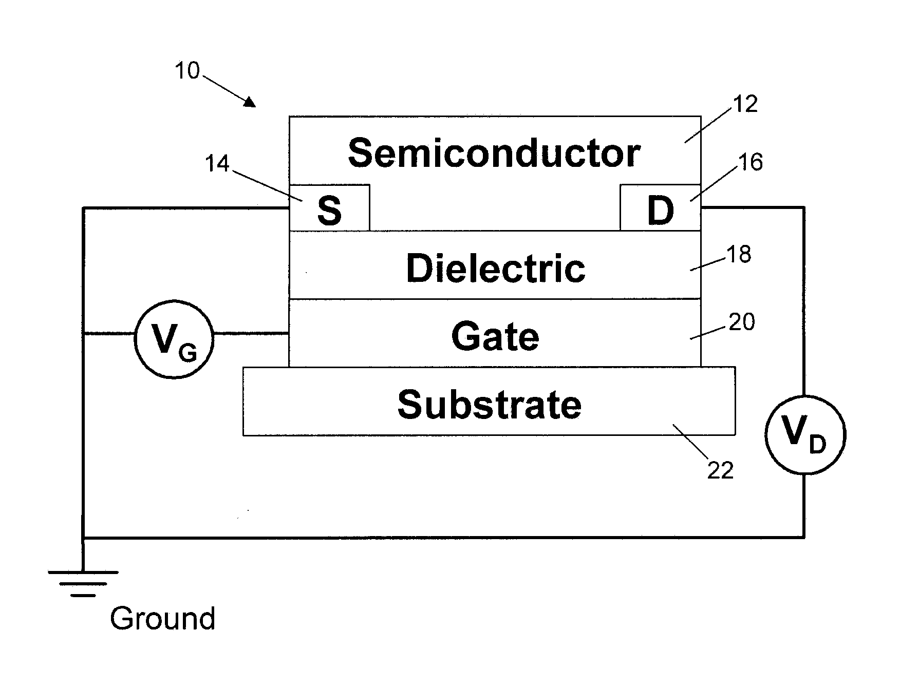
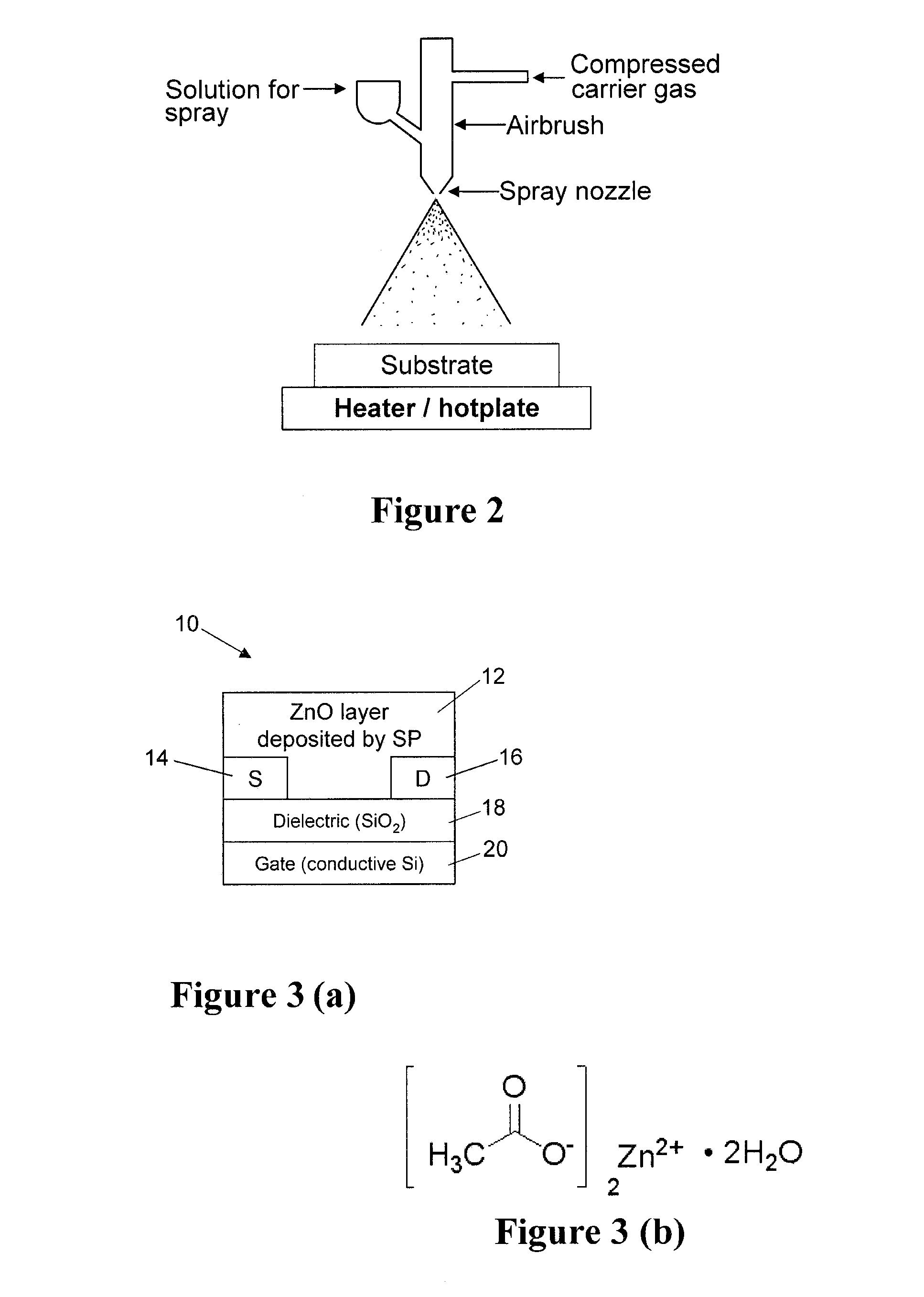
[0049]By way of introduction, as illustrated in FIG. 1, a bottom-gate bottom-contact TFT device 10 consists of a semiconducting active layer 12 applied onto a three-terminal electrode architecture comprising a source electrode 14, a drain electrode 16 and a gate electrode 20. The gate electrode 20 is separated from the semiconductor layer 12 and the source and drain electrodes by a dielectric layer 18. In embodiments of the present invention, the semiconducting layer 12 may be an oxide or oxide-based material, and is deposited using spray pyrolysis (which may be abbreviated to “SP” herein). As will be described in further detail below, alternative device architectures, other than bottom-gate bottom-contact devices, are also possible.

[0050]The embodiments of the invention seek to address both the issue ...


PUM

PropertyMeasurementUnit
temperatureaaaaaaaaaa
temperaturesaaaaaaaaaa
temperatureaaaaaaaaaa

Abstract

A thin-film field-effect transistor is formed by forming a dielectric layer adjacent a gate, forming a source region and a drain region, and forming a semiconductor layer on the dielectric layer. The semiconductor layer is deposited by spray pyrolysis and comprises a material selected from a group comprising: oxides; oxide-based materials; mixed oxides; metallic type oxides; group I-IV, II-VI, III-VI, IV-VI, V-VI and VIII-VI binary chalcogenides; and group I-II-VI, II-II-VI, II-III-VI, II-VI-VI and V-II-VI ternary chalcogenides.

Description

[0001]This invention relates to thin-film field-effect transistors and a fabrication method thereof.BACKGROUND TO THE INVENTION[0002]Semiconducting thin-film transistors (TFTs) comprise a substrate, a semiconducting layer, a dielectric layer, and conducting materials for the source, drain and gate electrodes. Depending on the gate potential (VG) and the drain potential (VD), the channel current (i.e. the current flowing from the source electrode to the drain electrode, often referred to as ID) can be modulated.[0003]Over the last ten years, TFTs based on amorphous inorganic semiconductors have become the key technology for numerous applications. The most notable example comes from the information display industry where amorphous (a-Si) transistors, in particular, are found at the heart of everyday products including electrophoretic displays (i.e. E-paper), liquid crystal displays (LCDs), liquid crystal on silicon (LCoS) for micro-display and projection TV technology, to name a few.[...

Claims


Application Information

Patent Timeline
Patent Type & Authority Applications(United States)
IPC IPC(8): H01L21/34
CPCH01L29/78681H01L27/1292H01L29/7869
Inventor ANTHOPOULOS, THOMASBRADLEY, DONAL DONAT CONORSMITH, JEREMY NICHOLAS
Owner IMPERIAL INNOVATIONS LTD
Why Eureka
Try Eureka