Semiconductor device

a semiconductor and device technology, applied in semiconductor devices, instruments, electrical equipment, etc., can solve the problems of increasing reducing productivity, so as to reduce the number of photomasks and the number of steps, the effect of processing the semiconductor region into an island-shaped semiconductor layer

Active Publication Date: 2012-03-15
SEMICON ENERGY LAB CO LTD
View PDF4 Cites 25 Cited by
  • Summary
  • Abstract
  • Description
  • Claims
  • Application Information

AI Technical Summary

Benefits of technology

[0017]A photolithography step for processing the semiconductor region into an island-shaped semiconductor layer can be reduced; thus, the number of photomasks and the number of steps can be reduced. Therefore, a semiconductor device, which can be manufactured with high productivity and high yield, can be provided.
[0018]In the above structure, the wiring whose potential is lower than those of the first wiring and the second wiring and the transistors in which the gate electrode layer is electrically connected to the source electrode layer are provided between the first wiring and the second wiring; thus, leakage current between the first wiring and the second wiring can be prevented in the case where a continuous oxide semiconductor film is provided above or below the adjacent wirings. Therefore, a highly reliable semiconductor device can be provided.

Problems solved by technology

However, there is a problem in that increase in photolithography steps involved in the photolithographic process causes increase in the number of photomasks and the number of steps, which results in high cost and decrease in productivity.

Method used


Image

  • Semiconductor device
  • Semiconductor device
  • Semiconductor device

Examples


embodiment 1

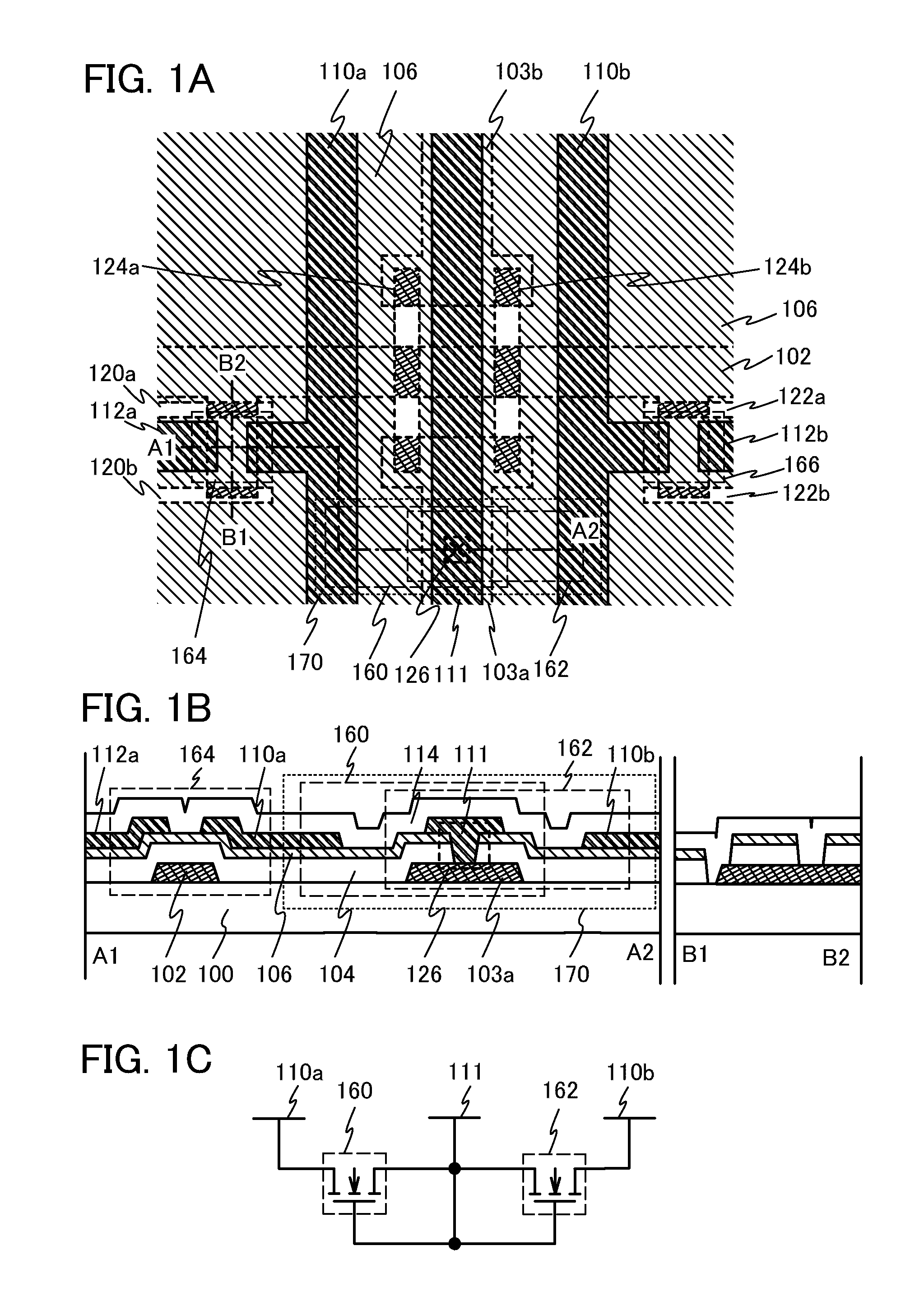
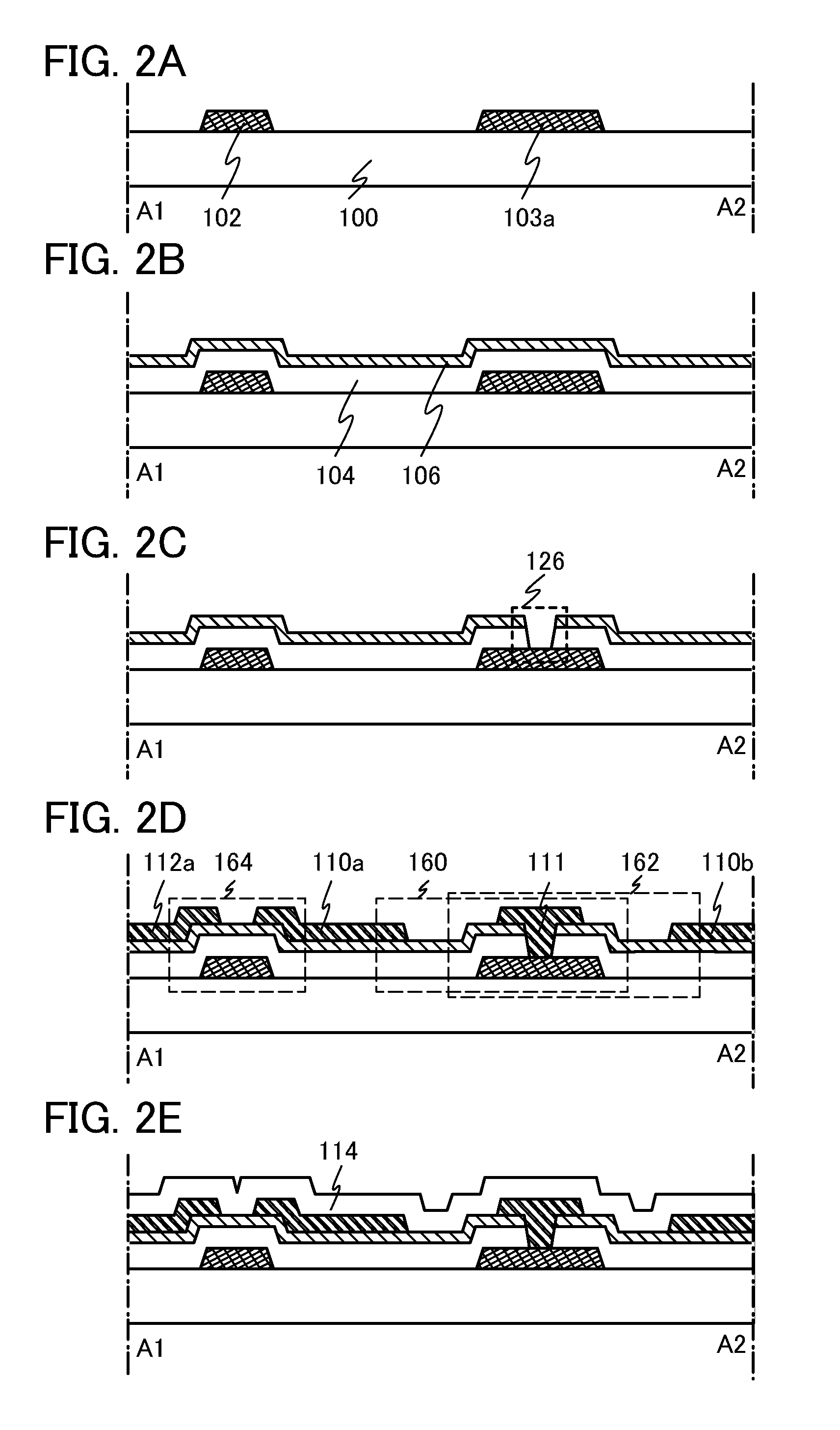
[0035]In this embodiment, a semiconductor device and a method for manufacturing the semiconductor device according to one embodiment of the present invention will be described with reference to FIGS. 1A to 1C and FIGS. 2A to 2E.

[0036]FIGS. 1A to 1C illustrate a semiconductor device according to one embodiment of the present invention. FIG. 1A is a plan view of the semiconductor device and FIG. 1B corresponds to a cross section along dashed-dotted line A1-A2 and dashed-dotted line B1-B2 in FIG. 1A. Further, FIG. 1C corresponds to an equivalent circuit of a region 170 in FIG. 1A.

[0037]The semiconductor device in FIGS. 1A and 1B includes a first wiring 110a, a second wiring 110b, and a third wiring 111 whose potential is lower than those of the first wiring 110a and the second wiring 110b between the first wiring 110a and the second wiring 110b. Further, the first wiring 110a is electrically connected to the third wiring 111 through an oxide semiconductor film 106 to which a gate elect...

embodiment 2

[0112]In this embodiment, an example of a liquid crystal display device is described as an example of a semiconductor device disclosed in this specification, with reference to FIGS. 3A and 3B, and FIG. 4. The same portion as or a portion having similar function to those described in Embodiment 1 can be formed in a manner similar to that described in Embodiment 1; therefore, repetitive description is omitted. In addition, detailed description of the same portions is not repeated.

[0113]FIG. 3A is a plan view of a liquid crystal display device and FIG. 3B is a cross-sectional view taken along dashed and dotted line C1-C2 and dashed-dotted line C3-C4 in FIG. 3A. Note that FIG. 3A is a plan view of a substrate 300 side where components up to a pixel electrode layer 307 are formed, and an insulating layer 306 and the like are omitted for simplification. FIG. 4 is an equivalent circuit diagram of a liquid crystal display device corresponding to FIGS. 3A and 3B.

[0114]FIGS. 3A and 3B illustr...

embodiment 3

[0129]In this embodiment, an example of a light-emitting display device is described as an example of a semiconductor device disclosed in this specification, with reference to FIGS. 5A and 5B, and FIG. 6. The same portion as or a portion having similar function to those described in Embodiment 1 can be formed in a manner similar to that described in Embodiment 1; therefore, repetitive description is omitted. In addition, detailed description of the same portions is not repeated.

[0130]FIG. 5A is a plan view of a light-emitting display device and FIG. 5B is a cross-sectional view taken along dashed and dotted line D1-D2 and dashed-dotted line D3-D4 in FIG. 5A. Note that FIG. 5A is a plan view of a substrate 200 side where components up to a pixel electrode layer 207 is formed, and an insulating layer 206 and the like are omitted for simplification. FIG. 6 is an equivalent circuit diagram of the light-emitting display corresponding to FIGS. 5A and 5B.

[0131]FIGS. 5 and 5B illustrate par...


PUM


Abstract

To provide a semiconductor device including a transistor formed using a highly reliable oxide semiconductor. To provide a semiconductor device which can be manufactured with high productivity and high yield by reducing the number of photolithography steps. The semiconductor device includes a first wiring, a second wiring, and a third wiring whose potential is lower than those of the first wiring and the second wiring between the first wiring and the second wiring. In the semiconductor device, the first wiring is electrically connected to the third wiring through a first transistor in which a gate electrode layer is electrically connected to a source electrode layer, the second wiring is electrically connected to the third wiring through a second transistor in which the gate electrode layer is electrically connected to the source electrode layer, and a continuous oxide semiconductor film used for a semiconductor region of the first transistor and the second transistor is provided above or below the first wiring, the second wiring, and the third wiring.

Description

BACKGROUND OF THE INVENTION[0001]1. Field of the Invention[0002]The present invention relates to a semiconductor device and a method for manufacturing the semiconductor device.[0003]In this specification, a semiconductor device generally means a device which can function by utilizing semiconductor characteristics, and an electrooptic device, a semiconductor circuit, and electronic equipment are all semiconductor devices.[0004]2. Description of the Related Art[0005]A technique by which transistors are formed using semiconductor thin films over a substrate having an insulating surface has been attracting attention. Such transistors are used in a wide range of electronic appliances such as an integrated circuit (IC) and an image display device (display device).[0006]As a material having semiconductor characteristics suitable for transistors, a metal oxide has attracted attention, and transistors in which a channel formation region is formed using such metal oxide having semiconductor c...

Claims


Application Information

Patent Timeline
Patent Type & Authority Applications(United States)
IPC IPC(8): H01L33/08
CPCH01L27/1225G02F1/13454H01L27/3262H01L27/1251H10K59/1213H01L27/124
Inventor MIYAKE, HIROYUKI
Owner SEMICON ENERGY LAB CO LTD
Why Eureka
Try Eureka