Manufacturing method and manufacturing device for electronic component

Active Publication Date: 2012-03-29
MURATA MFG CO LTD
View PDF3 Cites 5 Cited by
  • Summary
  • Abstract
  • Description
  • Claims
  • Application Information

AI Technical Summary

Benefits of technology

[0009]Preferred embodiments of the present invention provide a manufacturing method for an electronic component in which a portion of an outer electrode is located on the main surface of a dielectric block, the manufacturing method being capable of forming, with a high degree of accuracy, the portion of the outer electrode located on the main surface of the dielectric block.
[0011]In a preferred embodiment of the present invention, in the formation process, light irradiated from the first main surface side to the dielectric block is detected by a second detector disposed on the second main surface side, thereby detecting the positions of the first and second inner electrodes within the dielectric block, and a conductive layer is formed in a portion on the second main surface, determined based on the detection result of the second detector, thereby forming the second portion of each of the first and second outer electrodes. According to this configuration, it is also possible to form the second portion of each of the first and second outer electrodes with a high degree of accuracy.
[0012]In another preferred embodiment of the present invention, the dielectric block prepared in the preparation process preferably is a mother substrate in which a plurality of pairs of the first and second inner electrodes are formed in a matrix pattern, and the formation process includes a cutting process in which, after the conductive layer has been formed, the mother substrate is cut into a plurality of chips and the first portion of each of the first and second outer electrodes is formed from the conductive layer, and a process in which the third portion of each of the first and second outer electrodes is formed with respect to each of the plurality of chips. According to this configuration, it is possible to manufacture a plurality of electronic components simultaneously in parallel. Accordingly, it is possible to manufacture the plurality of electronic components in a short period of time with fewer processes.
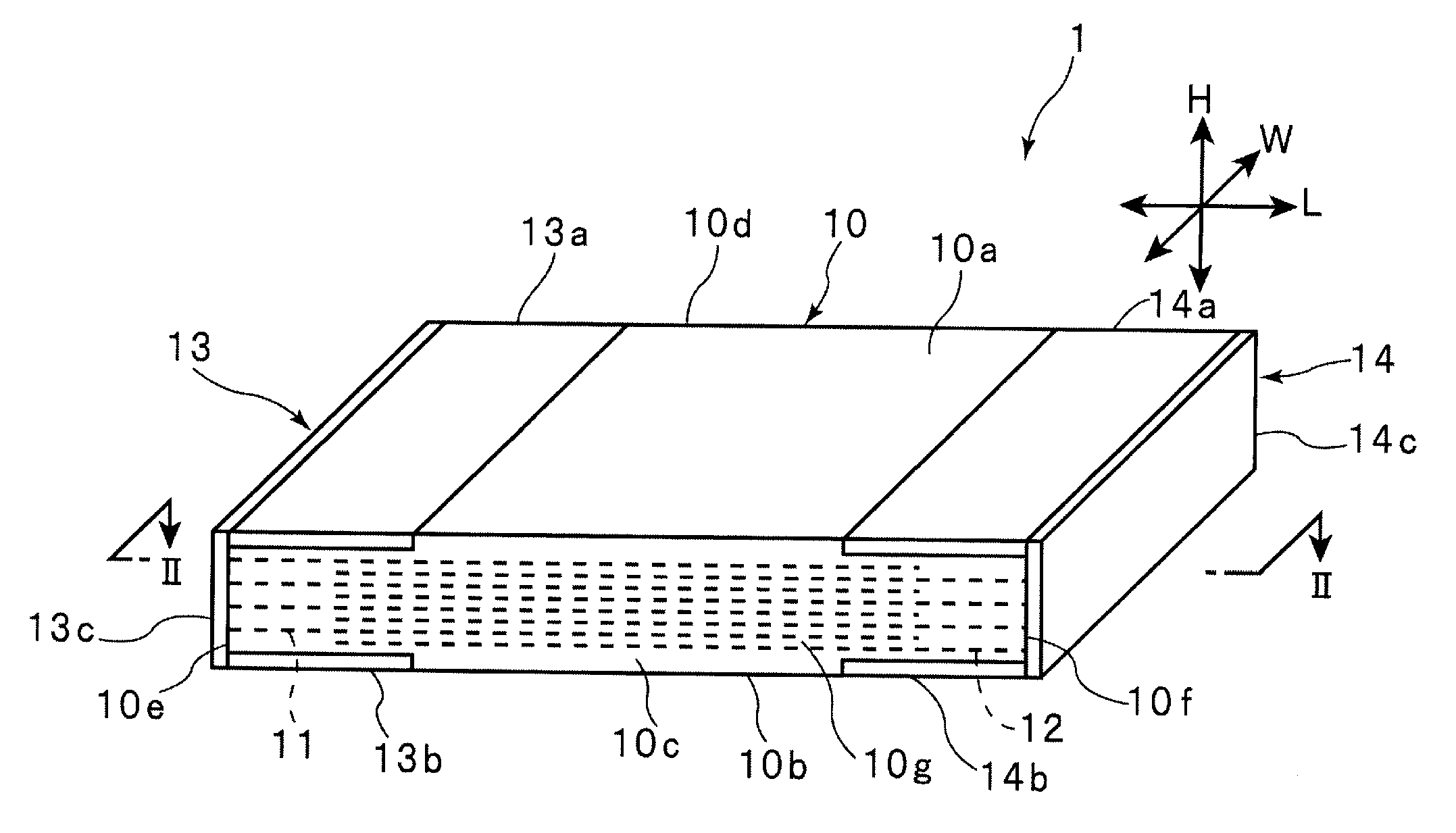
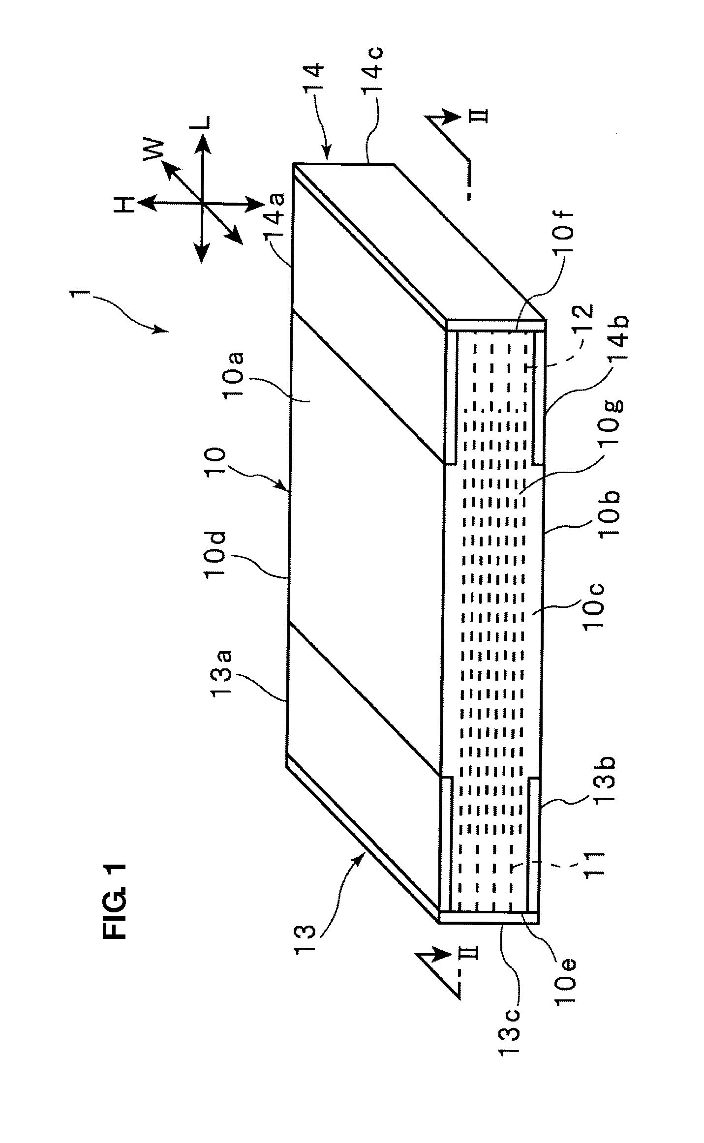
[0013]In another preferred embodiment of the present invention, the first portion of each of the first and second outer electrodes is formed throughout an entire region in the width direction of the dielectric block, and the conductive layer is formed in a stripe configuration along the width direction of the dielectric block. In this configuration, when the first and second conductive layers are formed, it is not necessary to consider a formation position in the width direction with respect to the inner electrode. Accordingly, it is easy to perform the positioning of the formation position.
[0014]Furthermore, in another preferred embodiment of the present invention, the conductive layer is formed through the use of a screen printing method, an ink-jet printing method, a gravure printing method, or a photolithography method, for example. When the ink-jet printing method is used for the formation of the conductive layer, no mask is necessary and it is possible to form the conductive layer with a high degree of accuracy. In addition, even if there are a concavity and a convexity on a formation surface, it is possible to apply the ink-jet printing method. When the gravure printing method is used for the formation of the conductive layer, it is possible to form the conductive layer at high speed. When the photolithography method is used for the formation of the conductive layer, it is possible to form the conductive layer with a high degree of accuracy.
[0016]In various preferred embodiments of the present invention, since the conductive layer is formed at a position determined based on the optically detected position of an inner electrode, it is possible to form the first portion of each of the first and second outer electrodes with a high degree of accuracy. Accordingly, it is possible to manufacture an electronic component in which the first portion of each of the first and second outer electrodes is accurately formed at the exact correct position.

Problems solved by technology

However, as described in Japanese Unexamined Patent Application Publication No. 8-236391, in the method in which the outer electrodes are formed by dipping the end portions of the dielectric block in conductive paste, since the portions of the outer electrodes located on the main surface of the dielectric block are formed by wetting of the end portions with conductive paste, it has been difficult to form the outer electrodes with a high degree of accuracy.

Method used


Image

  • Manufacturing method and manufacturing device for electronic component
  • Manufacturing method and manufacturing device for electronic component
  • Manufacturing method and manufacturing device for electronic component

Examples


Embodiment Construction

[0034]Hereinafter, preferred embodiments of the present invention will be described with reference to drawings, and hence the present invention will be clarified.

[0035]FIG. 1 is a schematic perspective view of an electronic component manufactured according to the present preferred embodiment of the present invention, and FIG. 2 is a schematic cross-sectional view when being cut along the length direction of the electronic component. First, with reference to FIG. 1 and FIG. 2, an electronic component will be described in detail that is manufactured by a manufacturing device for an electronic component according to the present preferred embodiment.

[0036]An electronic component 1 illustrated in FIG. 1 is a ceramic electronic component including a ceramic dielectric block 10 having optical transparency. For example, the electronic component 1 may be a ceramic capacitor, a ceramic piezoelectric element, a ceramic thermistor, a ceramic inductor, or other suitable electronic component, for...


PUM

PropertyMeasurementUnit
Electrical conductoraaaaaaaaaa
Widthaaaaaaaaaa

Abstract

A manufacturing method for an electronic component forms with a high degree of accuracy a portion of an outer electrode on a main surface of a dielectric block. Light irradiated from a second main surface side is detected by a detector disposed on a first main surface side, thereby detecting the positions of first and second inner electrodes, and a conductive layer is formed in a portion on a first main surface, determined based on the detection result by the detector, thereby forming first portions of individual first and second outer electrodes.

Description

BACKGROUND OF THE INVENTION[0001]1. Field of the Invention[0002]The present invention relates to a manufacturing method and a manufacturing device for an electronic component, and, in detail, relates to a manufacturing method and a manufacturing device for an electronic component in which a portion of an outer electrode is formed and located on a main surface.[0003]2. Description of the Related Art[0004]In recent years, for example, as an electronic component capable of being downsized, there has been widely used such a chip-type laminated ceramic electronic component as described in Japanese Unexamined Patent Application Publication No. 2007-294839. Usually, the chip-type laminated ceramic electronic component includes a dielectric block and a first outer electrode and a second outer electrode, provided on an end surface of the dielectric block. In view of the connectability between an electronic component and a substrate, usually, each of the first outer electrode and the second o...

Claims


Application Information

Patent Timeline
IPC IPC(8): H01G7/00H01G4/12H01G4/30H01G13/00
CPCH01F17/0013H01G4/0085H01G4/12Y10T29/435H01G4/30H01G13/006H01G4/232Y10T29/5313Y10T29/53217Y10T29/53243H01G4/248H01G13/00H05K3/12H05K13/00
Inventor TSUTSUMI, HIRONORI
Owner MURATA MFG CO LTD
Why Eureka
Try Eureka