Touchscreen panel input device manufacturing method, piezoelectric element and touchscreen panel input device

a touchscreen panel and input device technology, applied in the direction of generators/motors, instruments, other domestic objects, etc., can solve the problems of inability to support multi-touch detection, damage, and inability to use input tools other than fingers, etc., to achieve high transmittance and high transmittance

Inactive Publication Date: 2012-03-29
STANLEY ELECTRIC CO LTD
View PDF3 Cites 62 Cited by
  • Summary
  • Abstract
  • Description
  • Claims
  • Application Information

AI Technical Summary

Benefits of technology

[0022]According to the present invention, a method for manufacturing a touchscreen panel input device with high transmittance which can detect strength of a pushing pressure of a touch input in addition to detecting a touch position and provide a tactile feedback by generating oscillation locally at the touch position...

Problems solved by technology

Moreover, two transparent electrodes are contacted at the time of input operation to detect a position; therefore, it tends to be damaged by being worn down, and there is a problem in durability because the transparent conductive film must be deformed.
Furthermore, it is difficult to support multi-touch detection.
The capacitive-type touchscreen panel detects changes in capacitance when a finger contacts with the panel; therefore, input tools such as a pen, a stylus, etc. other than a finger cannot be used.
Structures of the surface acoustic wave type and the infrared scanning type touchscreen panels tend to be complicated, and it is difficult to support a multi-touch detection.
Moreover, none of the above types of touchscreen panels can detect a pushing force of an input operation of a user.
Those touchscreen panels just detect an input position on a panel but not a pushing pressure; therefore, it cannot be judged whether a user touches the position intentionally or unintentionally.
Furthermore, those touchscreen panels cannot feedback the input operation directly to the user.
In that case, the user needs to see the display device to confirm the input operation or the use...

Method used


Image

  • Touchscreen panel input device manufacturing method, piezoelectric element and touchscreen panel input device
  • Touchscreen panel input device manufacturing method, piezoelectric element and touchscreen panel input device
  • Touchscreen panel input device manufacturing method, piezoelectric element and touchscreen panel input device

Examples


Embodiment Construction

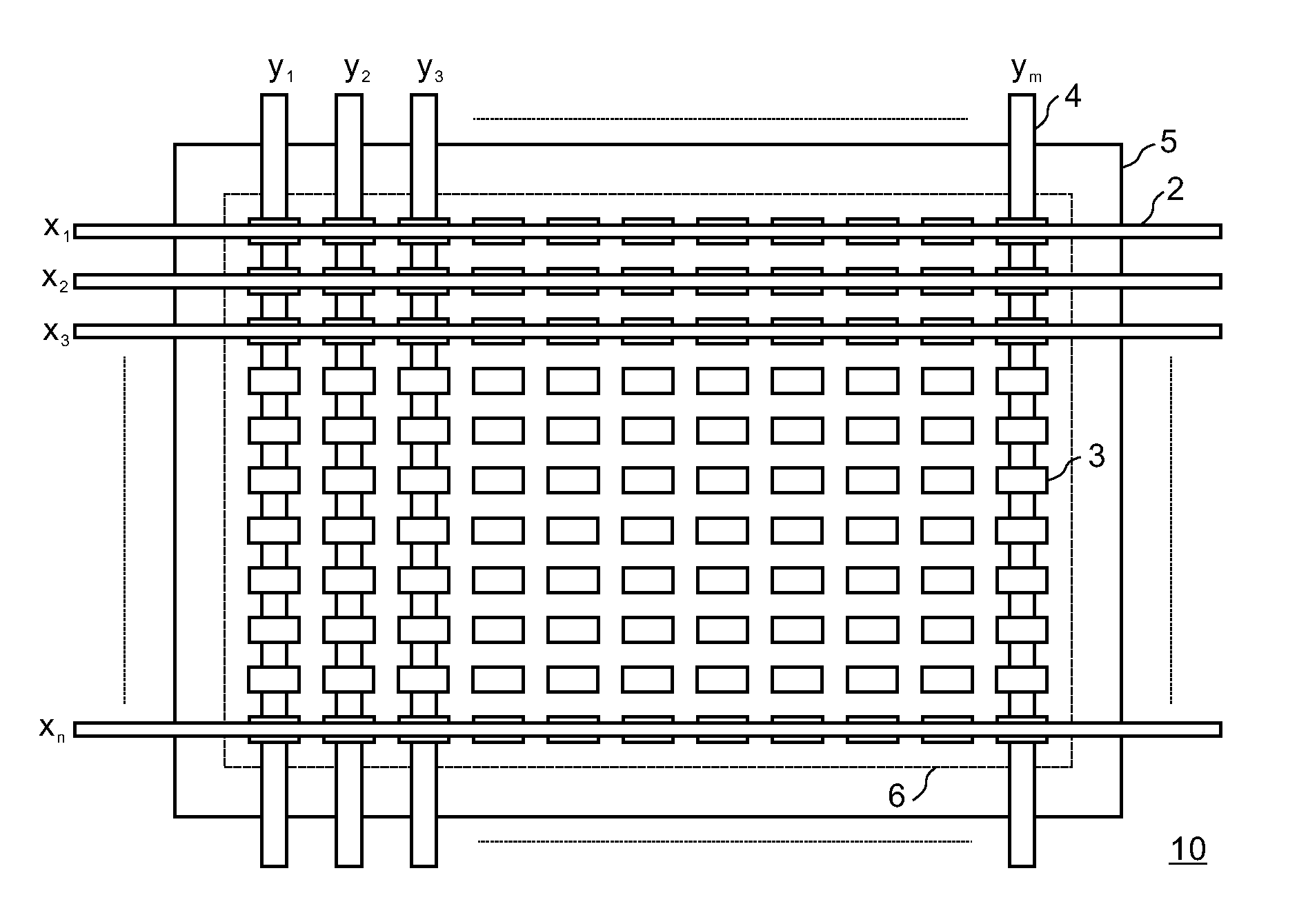
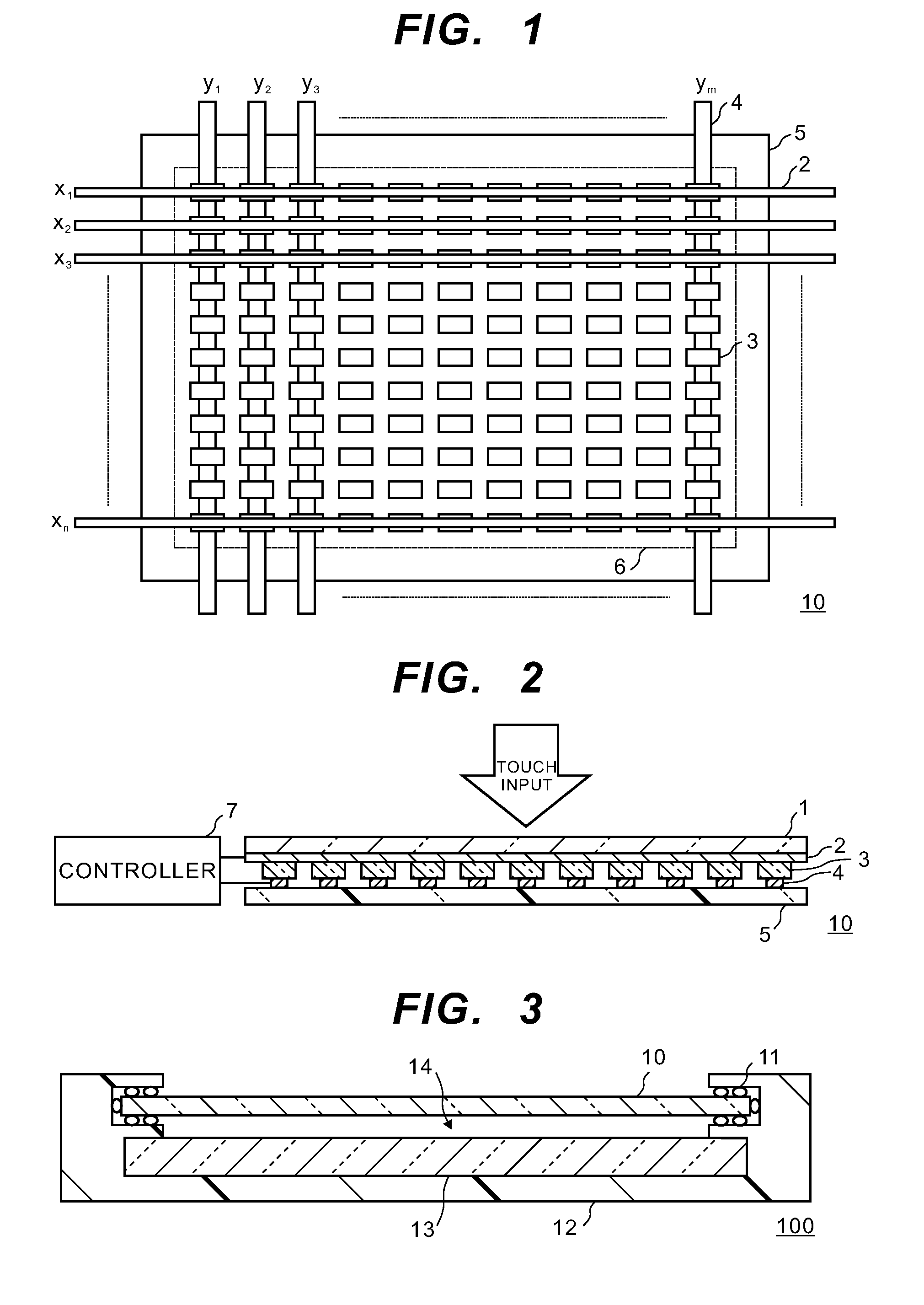
[0030]It has been well-known that lead perovskite oxide such as lead zirconate titanate (PZT) has high piezoelectricity. Comparing to polyvinylidene difluouride (PVDF), which is one of piezoelectric polymers, the PZT has piezoelectric constant (d31)=110 pm / V and electromechanical coupling factors (k)=0.6-0.8, which are performance indexes of electromechanical conversion, whereas the PVDF has lower indexes, that is, d31=20 pm / V and k=0.1. Therefore, it is understood that the lead perovskite oxide is more preferable for being used as an actuator than the piezoelectric polymer. However, the lead perovskite oxide has been used in an application as bulk ceramics but not in a sheet-type application or an application requiring transmittance.

[0031]Recently it becomes possible to form a thin film of the lead perovskite oxide which has similar piezoelectricity to bulk ceramics by solution coating, sputtering and ion-plating. The PZT thin film with a film thickness of 10-50 μm has 80% or more ...


PUM

PropertyMeasurementUnit
Pressureaaaaaaaaaa
Transparencyaaaaaaaaaa
Piezoelectricityaaaaaaaaaa

Abstract

A touchscreen panel input device is manufactured by forming a first adhesion layer and a second adhesion layer on a growth substrate, removing only the second adhesion layer from a selected region by irradiating laser, forming a growth base layer on the selected region where the second adhesion layer is removed and on the second adhesion layer and an oxide thin film having piezoelectricity on the growth base layer, transferring the oxide thin film layer on the selected region to a second substrate having first transparent electrodes by peeling-off, and adhering the second substrate to a third substrate having second transparent electrodes by placing the transferred oxide thin film layer between them. The touchscreen panel input device detects a pushing pressure in addition to a touch position with proving a tactile feedback.

Description

[0001]This application is based on Japanese Patent Application 2010-214944, filed on Sep. 27, 2010, the entire contents of which are incorporated herein by reference.BACKGROUND OF THE INVENTION[0002]A) Field of the Invention[0003]This invention relates to a method for manufacturing a touchscreen panel input device and to a piezoelectric element and a touchscreen panel input device manufactured by the method.[0004]B) Description of the Related Art[0005]Conventionally as an input method for a touchscreen panel, a resistive-type, a capacitive-type, a surface acoustic wave type, and an infrared scanning type have been known.[0006]A resistive touchscreen panel consists of a pair of facing substrates, that is, a flexible upper substrate which is an input panel surface and a lower substrate which faces the upper substrate. Inside each substrate is coated with a transparent conductive film, and the transparent conductive films are facing each other with a predetermined gap not to contact wi...

Claims


Application Information

Patent Timeline
IPC IPC(8): G06F3/041B32B38/10B32B37/14H01L41/047B32B37/02
CPCB32B37/02B32B38/0008B32B2309/105B32B2310/0843B32B2367/00B32B2457/208H01L41/331G06F3/041G06F3/0414G06F3/044G06F3/045H01L27/20H01L41/1132G06F3/016G06F3/04146H10N39/00H10N30/302H10N30/072H10N30/081
Inventor YASUDA, YOSHIAKI
Owner STANLEY ELECTRIC CO LTD
Why Eureka
Try Eureka