Laser processing method and method for manufacturing light-emitting device

a technology of laser processing and manufacturing method, which is applied in the field of laser processing method and manufacturing method of light-emitting device, can solve the problems of defective cutting, hard cutting of wafers with high precision, and the combination of blade dicing and diamond scribing incurs, so as to improve the precision of cutting wafers, reduce the force required for cutting wafers, and improve the effect of cutting wafers

Active Publication Date: 2012-03-29
HAMAMATSU PHOTONICS KK
View PDF4 Cites 22 Cited by
  • Summary
  • Abstract
  • Description
  • Claims
  • Application Information

AI Technical Summary

Benefits of technology

[0027]There is a case where it is preferred for the third step to be carried out after the fourth step. In this case, cutting the wafer from the second modified region acting as a start point before cutting the wafer from the first modified region acting as a start point can reduce the force required for cutting the wafer along the second line and improve the precision of cutting the wafer along the second line.
[0028]On the other hand, there is a case where it is preferred for the fourth step to be carried out after the third step. In this case, cutting the wafer from the first modified region acting as a start point before cutting the wafer from the second modified region acting as a start point can improve the precision of cutting the wafer along the first line while inhibiting the precision of cutting the wafer along the second line from decreasing.

Problems solved by technology

However, methods combining the blade dicing and diamond scribing incur the following problems.
When the single-crystal sapphire substrate is relatively thick, both faces of the wafer must be provided with scribe lines, whereby positional deviations between the scribe lines provided on both faces may result in defective cutting.
Therefore, using the blade dicing together with the diamond scribing causes a problem that the wafer is hard to cut with a high precision.
On the other hand, using the blade dicing alone takes an enormous time for incising the single-crystal sapphire substrate having a high hardness, while the blade wears out so much that it must be replaced frequently, which causes another problem that the manufacturing efficiency worsens.

Method used


Image

  • Laser processing method and method for manufacturing light-emitting device
  • Laser processing method and method for manufacturing light-emitting device
  • Laser processing method and method for manufacturing light-emitting device

Examples


Embodiment Construction

[0051]In the following, a preferred embodiment of the present invention will be explained in detail with reference to the drawings. The light-emitting device manufacturing method in accordance with this embodiment irradiates a wafer with a laser light which is transmitted through the front face of a substrate of the wafer, so as to form a modified region to become a cutting start point within the substrate of the wafer.

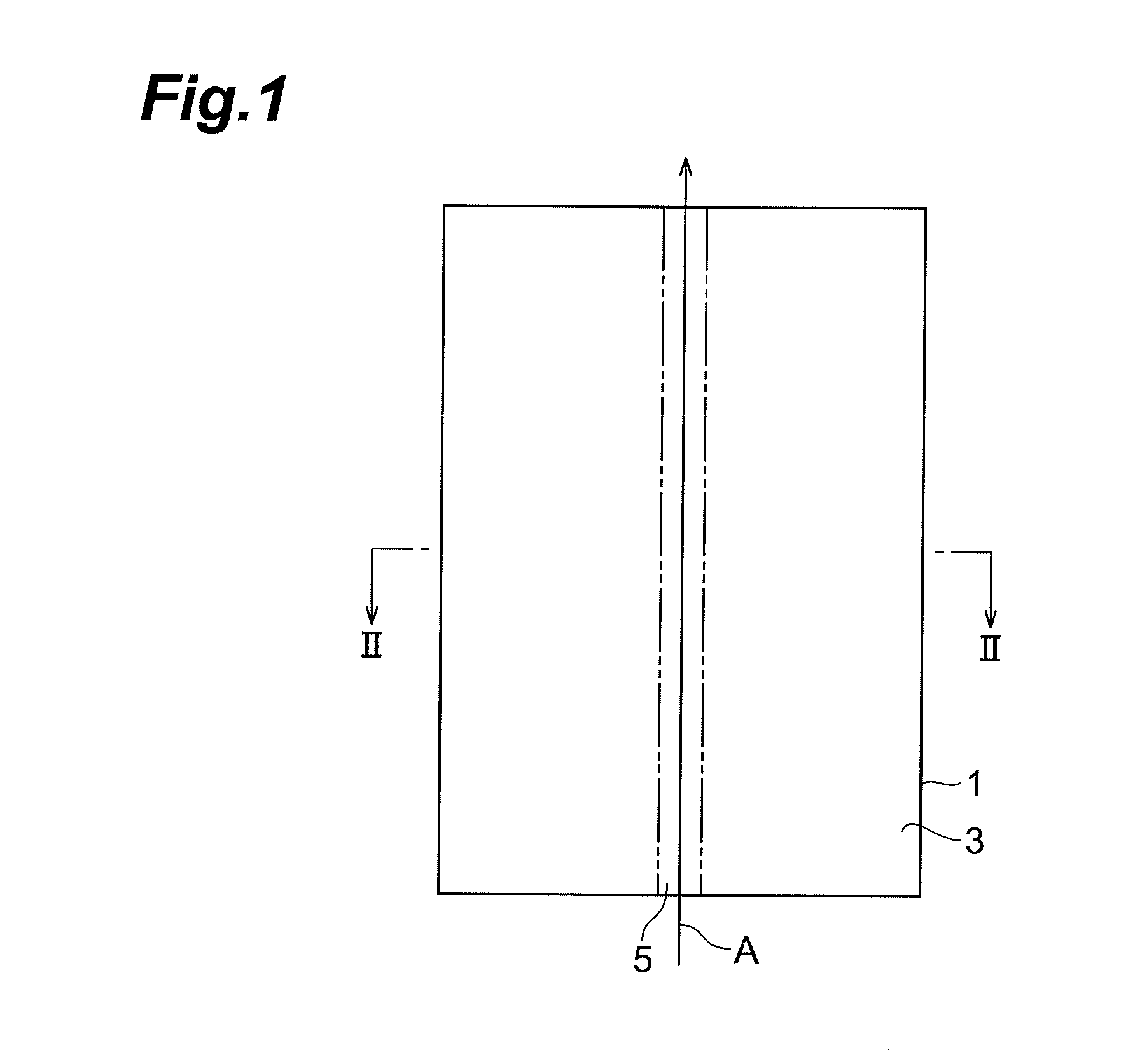
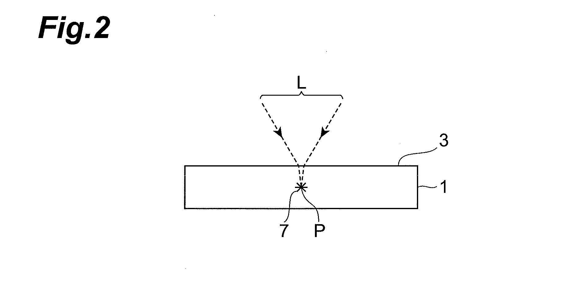
[0052]The principle of this laser processing will be explained with reference to FIGS. 1 to 6. FIG. 1 is a plan view of a substrate 1 during laser processing; FIG. 2 is a sectional view of the substrate 1 taken along the line II-II of FIG. 1; FIG. 3 is a plan view of the substrate 1 after the laser processing; FIG. 4 is a sectional view of the substrate 1 taken along the line IV-IV of FIG. 1; FIG. 5 is a sectional view of the substrate 1 taken along the line V-V of FIG. 1; and FIG. 6 is a plan view of the cut substrate 1.

[0053]As illustrated in FIGS. 1 and 2, a desira...


PUM

PropertyMeasurementUnit
angleaaaaaaaaaa
thicknessaaaaaaaaaa
thicknessaaaaaaaaaa

Abstract

A plurality of modified parts are formed at a first formation pitch for a line arranged along the M-plane of a single-crystal sapphire substrate to construct a modified region and cause a fracture occurring from the modified region to reach a principal surface of the single-crystal sapphire substrate. A plurality of modified parts are formed at a second formation pitch narrower than the first formation pitch for a line arranged along the A-plane of the single-crystal sapphire substrate to construct a modified region and cause a fracture occurring from the modified region to reach the principal surface of the single-crystal sapphire substrate. Along the lines, a knife edge is pressed against a wafer from the side of the single-crystal sapphire substrate opposite from the principal surface of the single-crystal sapphire substrate where the fractures have reached, to cut the wafer along the lines.

Description

CROSS-REFERENCE TO RELATED APPLICATIONS[0001]This application claims priority to Provisional Applications No. 61 / 387,173 filed on Sep. 28, 2010 and No. 61 / 490,926 filed on May 27, 2011 by the same Applicant, which are hereby incorporated by reference in their entirety.BACKGROUND OF THE INVENTION[0002]1. Field of the Invention[0003]The present invention relates to a laser processing method and a method for manufacturing a light-emitting device.[0004]2. Related Background Art[0005]Techniques for highly precisely cutting a wafer having a multilayer structure in which a semiconductor operation layer made of a group III-V compound semiconductor such as GaN is grown as a crystal on a single-crystal sapphire substrate have recently been demanded for manufacturing semiconductor light-emitting devices such as semiconductor laser devices and light-emitting diodes.[0006]For cutting a wafer having such a multilayer structure, blade dicing or diamond scribing has conventionally been used in gene...

Claims


Application Information

Patent Timeline
Patent Type & Authority Applications(United States)
IPC IPC(8): H01L33/08
CPCH01L33/0095B23K26/4075B23K26/0057B23K26/032B28D5/0011B23K26/0853B23K26/409B23K2201/40B23K26/063B23K26/40B23K26/0622B23K26/53B23K2101/40B23K2103/172B23K2103/50
Inventor YAMADA, TAKESHIHOSHIKAWA, MASAHARUNARA, YASUNAGA
Owner HAMAMATSU PHOTONICS KK
Why Eureka
Try Eureka