Heterogeneous substrate, nitride-based semiconductor device using same, and manufacturing method thereof

a technology of heterogeneous substrates and semiconductor devices, applied in the field of semiconductor devices, can solve the problems of reducing quantum efficiency, difficult to develop devices for long-wavelengths, and the inability to manufacture and commercialize nitride-based single crystal layers as substrates

Active Publication Date: 2012-04-12
KOREA ELECTRONICS TECH INST
View PDF15 Cites 6 Cited by
  • Summary
  • Abstract
  • Description
  • Claims
  • Application Information

AI Technical Summary

Benefits of technology

[0017]According to the present invention, it is possible to form a non-polar or semi-polar plane nitride layer having a flat surface and a small amount of internal defects on a non-polar or semi-polar plane of a base substrate by adjusting a crystal growth mode. Specifically, a nucleation layer is formed on the base substrate, a first buffer layer is formed on the nucleation layer such that the first buffer layer is grown faster in the vertical direction than in the lateral direction, a lateral growth layer is formed on the first buffer layer such that the lateral growth layer is grown faster in the lateral direction than in the vertical direction, and then a second buffer layer is formed on the lateral growth layer, to thereby form the non-polar or semi-polar plane nitride layer having a flat surface and a small amount of internal defects on the non-polar or semi-polar plane of the base substrate.
[0018]In particular, a silicon nitride layer having a plurality of holes is formed between the lateral growth layer on the first buffer layer and the second buffer layer, and then crystals are grown through portions exposed through the holes of the silicon nitride layer. Accordingly, growth of crystals in the lateral direction is promoted so as to form an a-plane nitride layer having a flat surface and a small amount of internal defects.

Problems solved by technology

In the case of a c-plane GaN / AlGaN / InGaN heterostructure, for example, a strong electric field generated by spontaneous polarization or piezoelectric polarization tilts the electronic band structure in the heterostructure so as to reduce a carrier recombination rate, resulting in a reduction in quantum efficiency.
This makes it difficult to develop devices for long-wavelengths.
The non-polar plane nitride-based single crystal layer cannot be manufactured and commercialized as a substrate although it has many advantages over the c-plane crystal layer because it is difficult to obtain a smooth surface and the non-polar plane nitride-based single crystal film has a large amount of internal defects compared to the c-plane crystal layer.
When this a-plane nitride-based single crystal is grown into a thick film or thin film, a film having no coalescence of ridges is formed to result in generation of a large amount of defects in the film.
Poor surface shapes and defects make it difficult to manufacture devices and they are present on the surface of a substrate so as to deteriorate the performance of a final thin film device.

Method used


Image

  • Heterogeneous substrate, nitride-based semiconductor device using same, and manufacturing method thereof
  • Heterogeneous substrate, nitride-based semiconductor device using same, and manufacturing method thereof
  • Heterogeneous substrate, nitride-based semiconductor device using same, and manufacturing method thereof

Examples


Embodiment Construction

[0041]The present invention will now be described more fully with reference to the accompanying drawings, in which exemplary embodiments of the invention are shown.

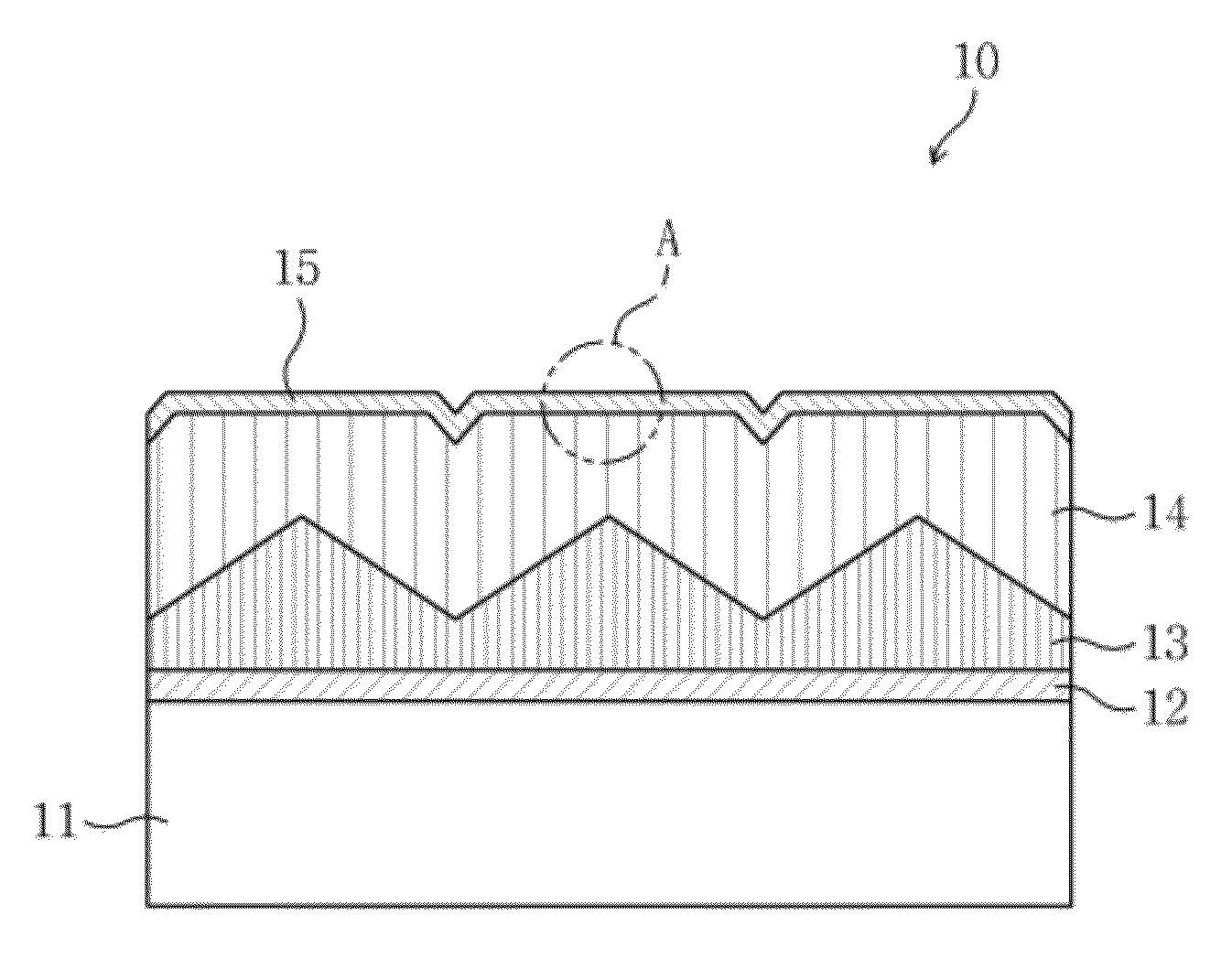
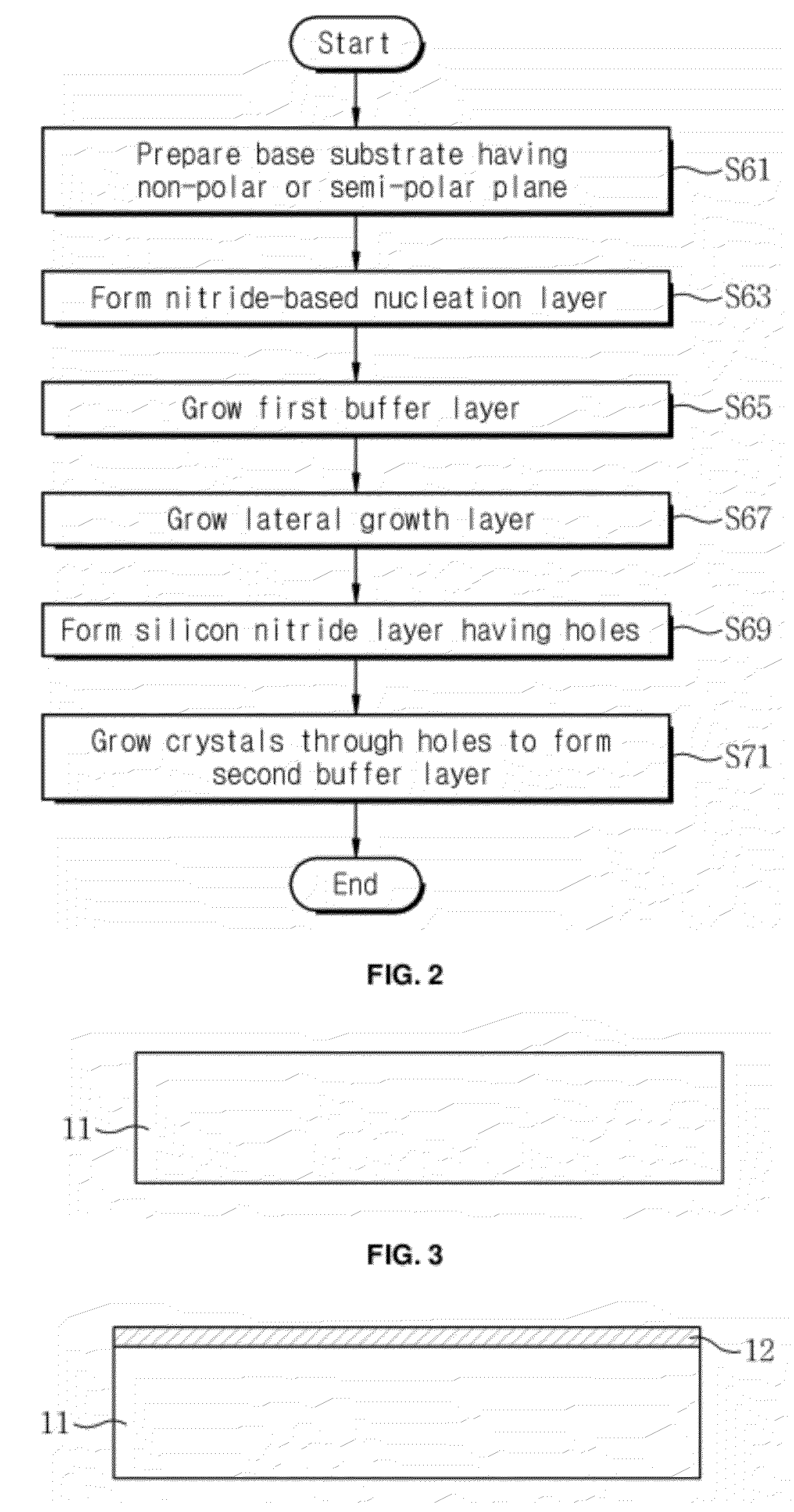
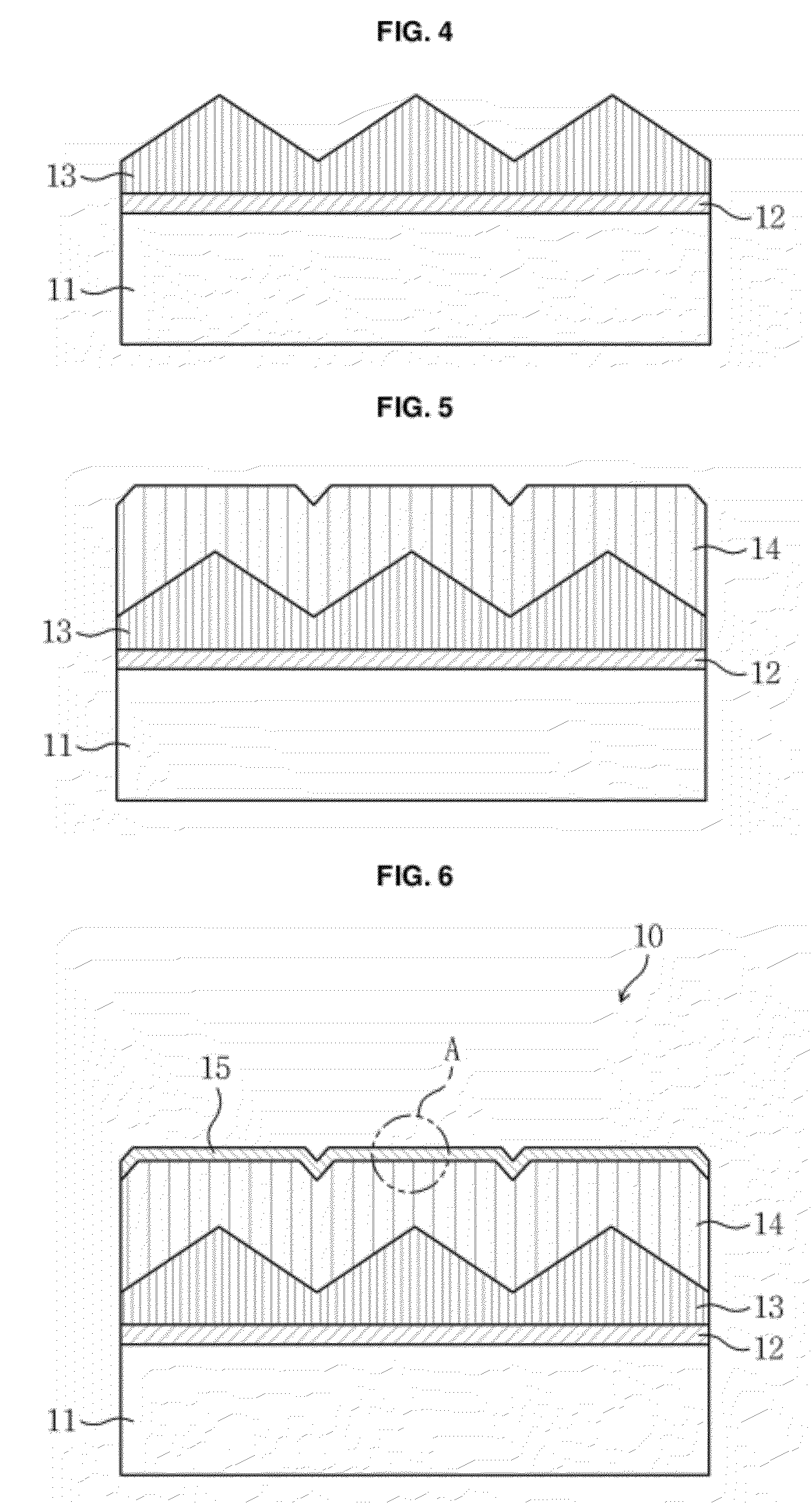
[0042]A method for manufacturing a heterogeneous substrate on which a nitride is deposited according to an embodiment of the present invention will be explained with reference to FIGS. 1 to 8. FIG. 1 is a flowchart illustrating the method for manufacturing a heterogeneous substrate on which a nitride is deposited according to an embodiment of the present invention and FIGS. 2 to 8 are views showing respective steps of the manufacturing method shown in FIG. 1.

[0043]Referring to FIG. 2, a base substrate 11 having one of a non-polar plane and a semi-polar plane is prepared (S61). A sapphire board may be used as the base substrate 11, and a SiC, ZnO or Si substrate may also be used. Here, planes other than c-plane, that is, a-plane, r-plane, m-plane, etc. can be used as the non-polar or semi-polar plane. In the current embodi...


PUM


Abstract

Provided are a heterogeneous substrate, a nitride-based semiconductor device using the same, and a manufacturing method thereof to form a high-quality non-polar or semi-polar nitride layer on a non-polar or semi-polar plane of the heterogeneous substrate by adjusting a crystal growth mode. A base substrate having one of a non-polar plane and a semi-polar plane is prepared, and a nitride-based nucleation layer is formed on the plane of the base substrate. A first buffer layer is grown faster in the vertical direction than in the lateral direction on the nucleation layer. A lateral growth layer is grown faster in the lateral direction than in the vertical direction on the first buffer layer. A second buffer layer is formed on the lateral growth layer. A silicon nitride layer having a plurality of holes may be formed between the lateral growth layer on the first buffer layer and the second buffer layer.

Description

TECHNICAL FIELD[0001]The present invention relates to a semiconductor device and a manufacturing method thereof, and more particularly, to a heterogeneous substrate formed in such a manner that a high-quality non-polar or semi-polar nitride layer is formed on a non-polar or semi-polar plane of a heterogeneous board such as a sapphire board by adjusting a growth control mode, a nitride-based semiconductor device using the same, and a manufacturing method thereof.BACKGROUND ART[0002]Most nitride-based single crystal semiconductor substrates such as GaN, used as a base when a semiconductor device is manufactured, are c-plane ({0001} plane) nitride thin films and are obtained by growing a nitride on a c-plane ({0001} plane) of a sapphire board through Metal Organic Chemical Vapor Deposition (MOCVD), Molecular Beam Epitaxy (MBE) or Hydride Vapor Phase Epitaxy (HVPE).[0003]A c-plane nitride-based single crystal layer formed in this manner has polarity since gallium and nitrogen, for examp...

Claims


Application Information

Patent Timeline
Patent Type & Authority Applications(United States)
IPC IPC(8): H01L29/22H01L21/20H01L29/06
CPCH01L21/0237H01L21/02458H01L21/02488H01L33/22H01L21/0254H01L21/02639H01L33/007H01L21/02502
Inventor HWANG, SUNG MINBAIK, KWANG HYEONSEO, YONG GONYOON, HYUNG DOPARK, JAE HYOUN
Owner KOREA ELECTRONICS TECH INST
Why Eureka
Try Eureka