Light-emitting diode having a wavelength conversion material layer, and method for fabricating same

a technology of wavelength conversion material and light-emitting diodes, which is applied in semiconductor/solid-state device manufacturing, electrical equipment, semiconductor devices, etc., can solve the problems of insufficient light for exciting the wavelength conversion material on the side of the light-emitting diode, and the light emitted from the light-emitting diode may have non-uniform color temperature distribution for each orientation angle, so as to improve the light extraction efficiency

Inactive Publication Date: 2012-04-12
KOREA PHOTONICS TECH INST
View PDF12 Cites 17 Cited by
  • Summary
  • Abstract
  • Description
  • Claims
  • Application Information

AI Technical Summary

Benefits of technology

[0029]As described above, the light-emitting diode according to the present invention comprises the wavelength conversion material layer containing the wavelength conversion material formed over the area, into which light emitted from the light-emitting area of the light-emitting diode chip can penetrate, and thus the light emitted from the light-emitting area of the light-emitting diode chip can excite the wavelength conversion material to a certain level.
[0030]As a result, since the wavelength conversion material proportional to the amount of emitted light or the intensity of emitted light passes through the path of light emitted from the light-emitting area of the light-emitting diode, the amount of light energy emitted from the wavelength conversion material and the amount of light energy emitted from the light-emitting diode are mixed in an appropriate ratio, and thus the color temperature distribution for each orientation angle can be uniform. Moreover, when the protective layer having a uniform thickness from the top of the light-emitting area of the light-emitting diode chip or from the light-emitting diode chip is disposed on the light-emitting diode chip and the wavelength conversion material layer is disposed thereon, it is possible to prevent the wavelength conversion material layer from absorbing and scattering light, thereby improving the light extraction efficiency.
[0031]Furthermore, according to an encapsulation process of a conventional method for fabricating a light-emitting diode, an encapsulating material mixed with a wavelength conversion material is deposited on the light-emitting diode by dispensing. However, according to the light-emitting diode of the present invention, it is not necessary to employ the encapsulation process using the wavelength conversion material such as a fluorescent material, and thus it is possible to overcome the failures associated with the fluorescent material such as the shift of color coordinates.

Problems solved by technology

When the wavelength conversion material is formed into a uniform thickness on the light-emitting diode, the amount of wavelength conversion material formed on the upper surface of the light-emitting diode may be smaller than the ability of light to excite the wavelength conversion material, and the amount of light for exciting the wavelength conversion material may be insufficient in the side of the light-emitting diode.
As a result, the light emitted from the light-emitting diode may have non-uniform color temperature distribution for each orientation angle.

Method used


Image

  • Light-emitting diode having a wavelength conversion material layer, and method for fabricating same
  • Light-emitting diode having a wavelength conversion material layer, and method for fabricating same
  • Light-emitting diode having a wavelength conversion material layer, and method for fabricating same

Examples


Embodiment Construction

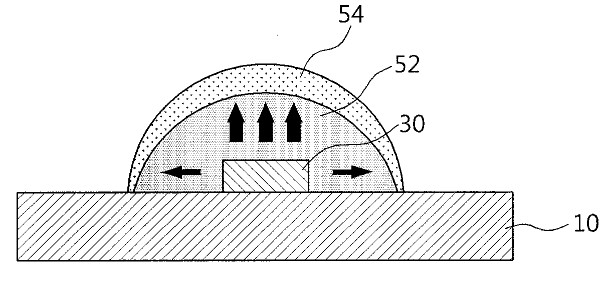
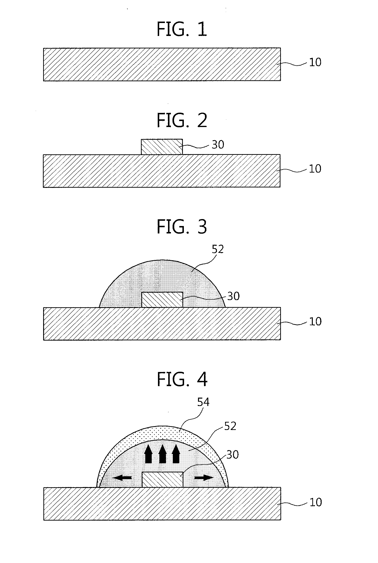
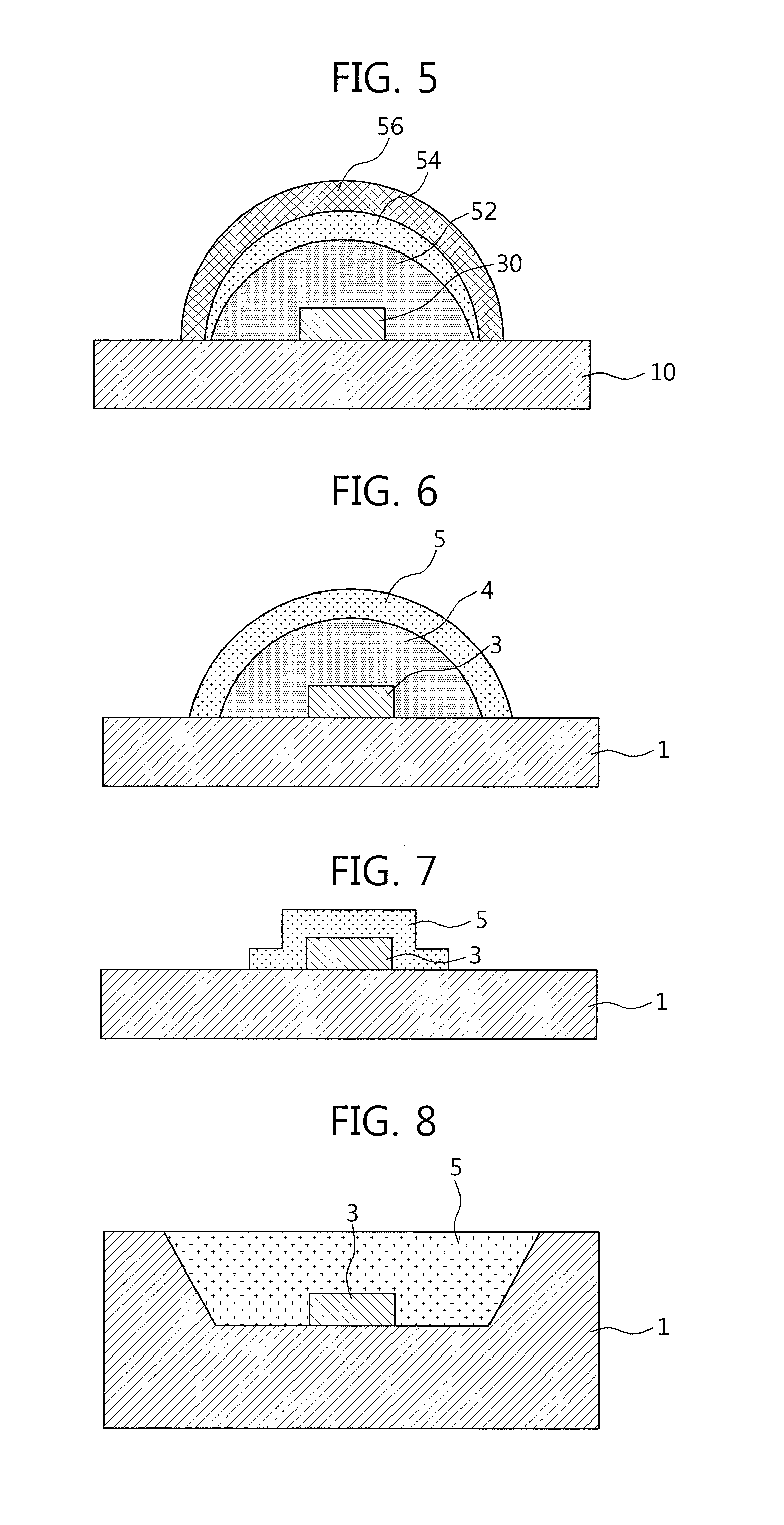
[0042]While the invention is susceptible to various modifications and alternative forms, specific embodiments thereof are shown by way of example in the drawings and will herein be described in detail. It should be understood, however, that there is no intent to limit the invention to the particular forms disclosed, but on the contrary, the invention is to cover all modifications, equivalents, and alternatives falling within the spirit and scope of the invention. Like numbers refer to like elements throughout the description of the figures.

[0043]It will be understood that, although the terms first, second, A, B etc. may be used herein to describe various elements, these elements should not be limited by these terms. These terms are only used to distinguish one element from another. For example, a first element could be termed a second element, and similarly, a second element could be termed a first element, without departing from the scope of the present invention. As used herein, t...


PUM


Abstract

Provided is a light-emitting diode having a wavelength conversion material and a method for fabricating the same. The light-emitting diode comprises: a base structure; a light-emitting diode chip arranged on the base structure; and a wavelength conversion material layer arranged on the light-emitting diode chip, such that the area adjacent the upper surface of the light-emitting diode chip is thicker than the area adjacent to the side surface of the light-emitting diode chip. In addition, the method for fabricating a light-emitting diode comprises: a step of arranging the light-emitting diode chip on the base structure; and a step of arranging a wavelength conversion material layer containing a light-transmitting photocurable material on the light-emitting diode chip, such that the area thereof adjacent to the upper surface of the light-emitting diode chip is thicker than the area thereof adjacent to the side surface of the light-emitting diode chip.

Description

TECHNICAL FIELD[0001]The present invention relates to a light-emitting diode and, more particularly, to a light-emitting diode having a wavelength conversion material layer and a method for fabricating the same.BACKGROUND ART[0002]A light-emitting diode (LED) is a semiconductor device that converts current into light and is mainly used as a light source of a display device. The light-emitting diode has excellent characteristics such as extremely small size, low power consumption, long life span, high response speed, etc. compared to existing light sources. Moreover, the light-emitting diode does not emit harmful electromagnetic waves such as ultraviolet rays and does not use mercury and other discharging gases, and thus is environmentally friendly.[0003]Among them, a white light-emitting diode is advantageous for miniaturization and high efficiency and has a long life span, compared to conventional light bulbs, and thus has been extensively studied. The white light-emitting diode is...

Claims


Application Information

Patent Timeline
Patent Type & Authority Applications(United States)
IPC IPC(8): H01L33/50
CPCH01L33/501H01L33/507H01L2933/0041H01L2924/0002H01L2924/00
Inventor LEE, KWANG-CHEOLKIM, JAE-PILSONG, SANG-BINKIM, SANG-MOOK
Owner KOREA PHOTONICS TECH INST
Why Eureka
Try Eureka