Photomultiplier tube

Active Publication Date: 2012-04-19
HAMAMATSU PHOTONICS KK
View PDF0 Cites 5 Cited by
  • Summary
  • Abstract
  • Description
  • Claims
  • Application Information

AI Technical Summary

Benefits of technology

[0007]Under the above-described circumstances, the present invention has been made in view of the above problem, an object of which is to provide a photomultiplier tube capable of suppressing a decrease in withstand voltage even when it is downsized.
[0009]According to the above-described photomultiplier tube, incident light is made incident onto the photocathode, thereby converted to photoelectrons, the photoelectrons are made incident onto the electron multiplying part formed with a plurality of stages of dynodes on the inner surface of the first substrate inside the housing and then multiplied accordingly, and the multiplied electrons are taken out from the anode part as an electric signal. Here, each of the dynodes is provided at an end part on the side of the first substrate with a supporting base, a power supplying member extending to the second substrate which opposes the first substrate from the first end part thereof is electrically connected to the supporting base, and the power supplying member is connected to the power supplying part installed on the inner surface of the second substrate, thereby power is supplied to each of the dynodes. Further, the supporting base is formed in such a manner that the both end parts thereof are joined to the opposing surface of the first substrate, the central part thereof is spaced away from the opposing surface and a cross sectional area along the opposing surface at the first end part on the side of the power supplying member is made greater than a cross sectional area at the second end part. Thereby, at a region of an electron multiplying channel where the insulating surface of the substrate easily takes charge by secondary electrons incident thereon, etc., which are made incident, each of the dynodes is spaced away from the insulating surface of the substrate. It is, therefore, possible to suppress a decrease in withstand voltage. Still further, the end part of the supporting base on the side of a site in contact with the power supplying part of the substrate is increased in strength, by which the electron multiplying part is secured for physical strength when pressure is applied due to contact for supplying power. It is, thus, possible to suppress a decrease in withstand voltage without deformation, breakage, etc.
[0010]It is preferable that a recessed part is formed on the opposing surface of the first substrate and the central part of the supporting base is arranged over the recessed part, thereby being spaced away from the opposing surface. In this instance, since the central part of the supporting base can be spaced away from the substrate without any decrease in strength of the electron multiplying part, it is possible to further suppress a decrease in withstand voltage.
[0011]It is also preferable that the recessed part is formed so as to be astride a plurality of supporting bases connected individually to the plurality of stages of dynodes. The above-described constitution makes it possible to further suppress a decrease in withstand voltage by preventing electric charge due to secondary electrons passing between the plurality of stages of dynodes.
[0012]Further, it is also preferable that the plurality of supporting bases corresponding to the plurality of stages of dynodes are arranged in such a manner that the one end part and the other end part are alternately placed along the opposing surface of the first substrate. When they are placed in the above-described manner, it is possible to increase a cross sectional area along the substrate at the end part of each of the supporting bases on the side of the power supplying member. Therefore, the electron multiplying part can be further increased in physical strength to suppress a decrease in withstand voltage.

Problems solved by technology

However, in the above-described conventional photomultiplier tube, since structures different in potential are arranged in close proximity to each other on an insulating substrate, there is found a decrease in withstand voltage between the structures when the photomultiplier tube is downsized, and this is a problem.
Therefore, the dynodes are deformed or broken due to connection of power supplying members, and there is also a concern that the withstand voltage is decreased.

Method used


Image

  • Photomultiplier tube
  • Photomultiplier tube
  • Photomultiplier tube

Examples


Embodiment Construction

[0026]Hereinafter, a detailed description will be given for preferred embodiments of the photomultiplier tube related to the present invention by referring to drawings. In addition, in describing the drawings, the same or corresponding parts will be given the same reference numerals to omit overlapping description.

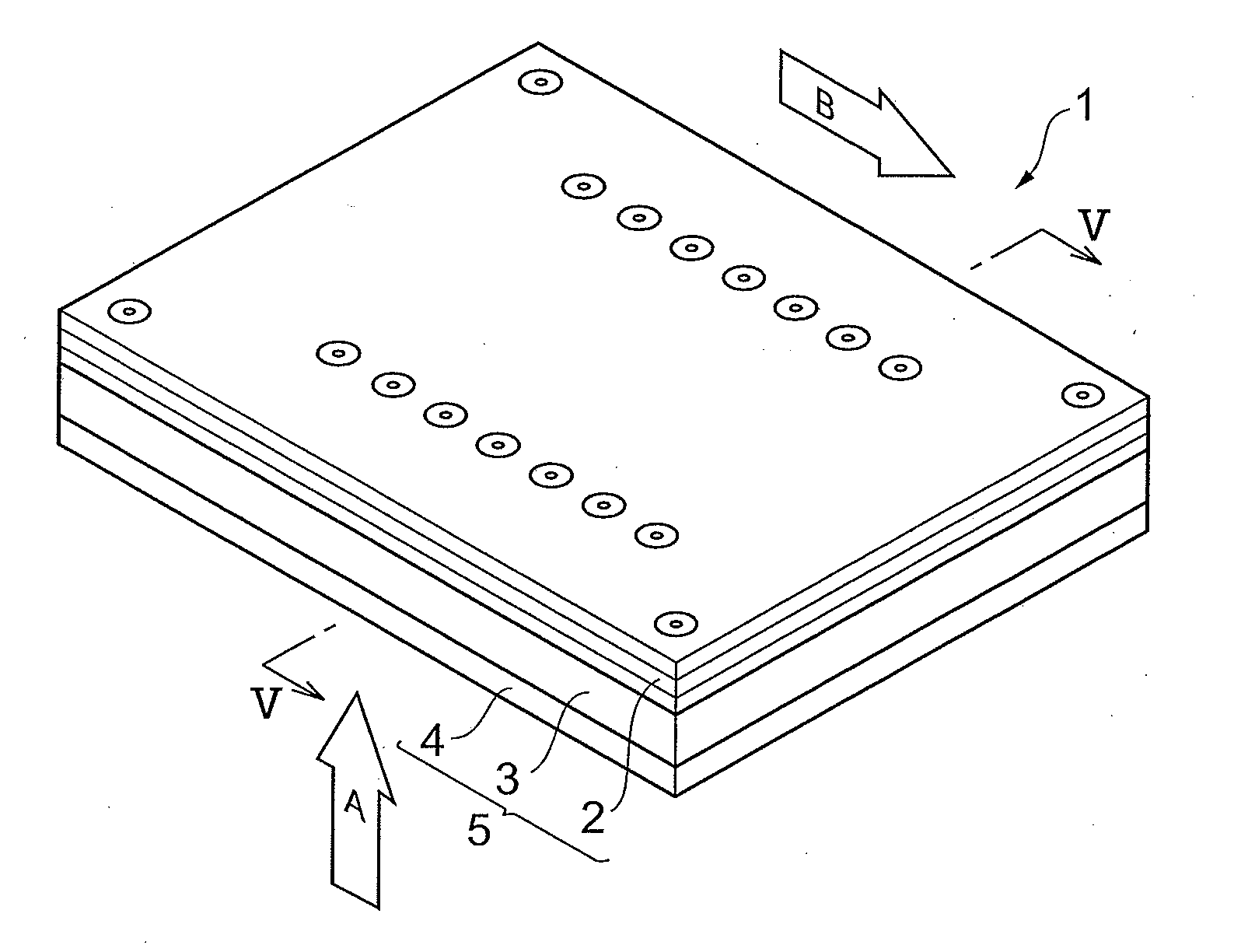
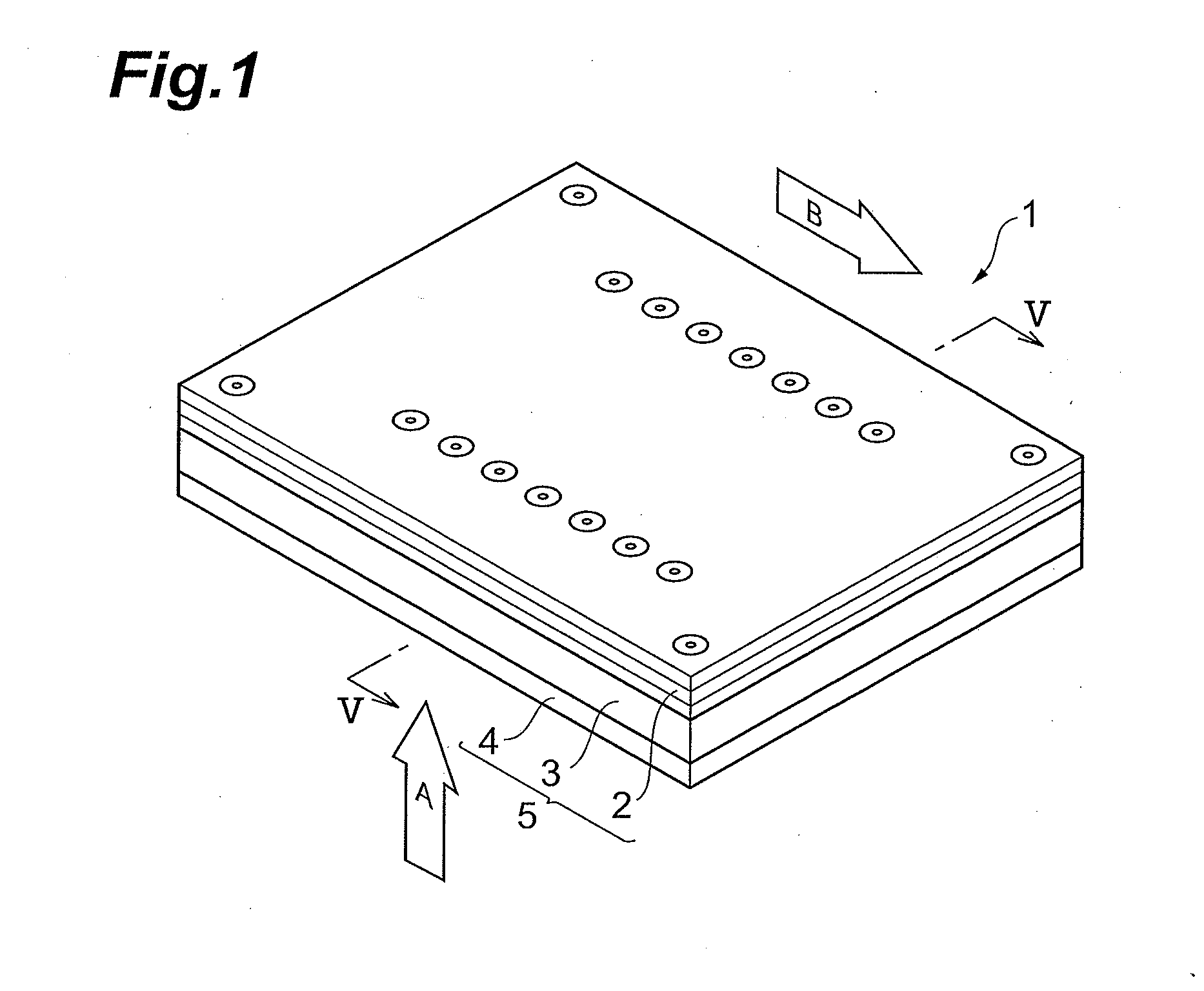
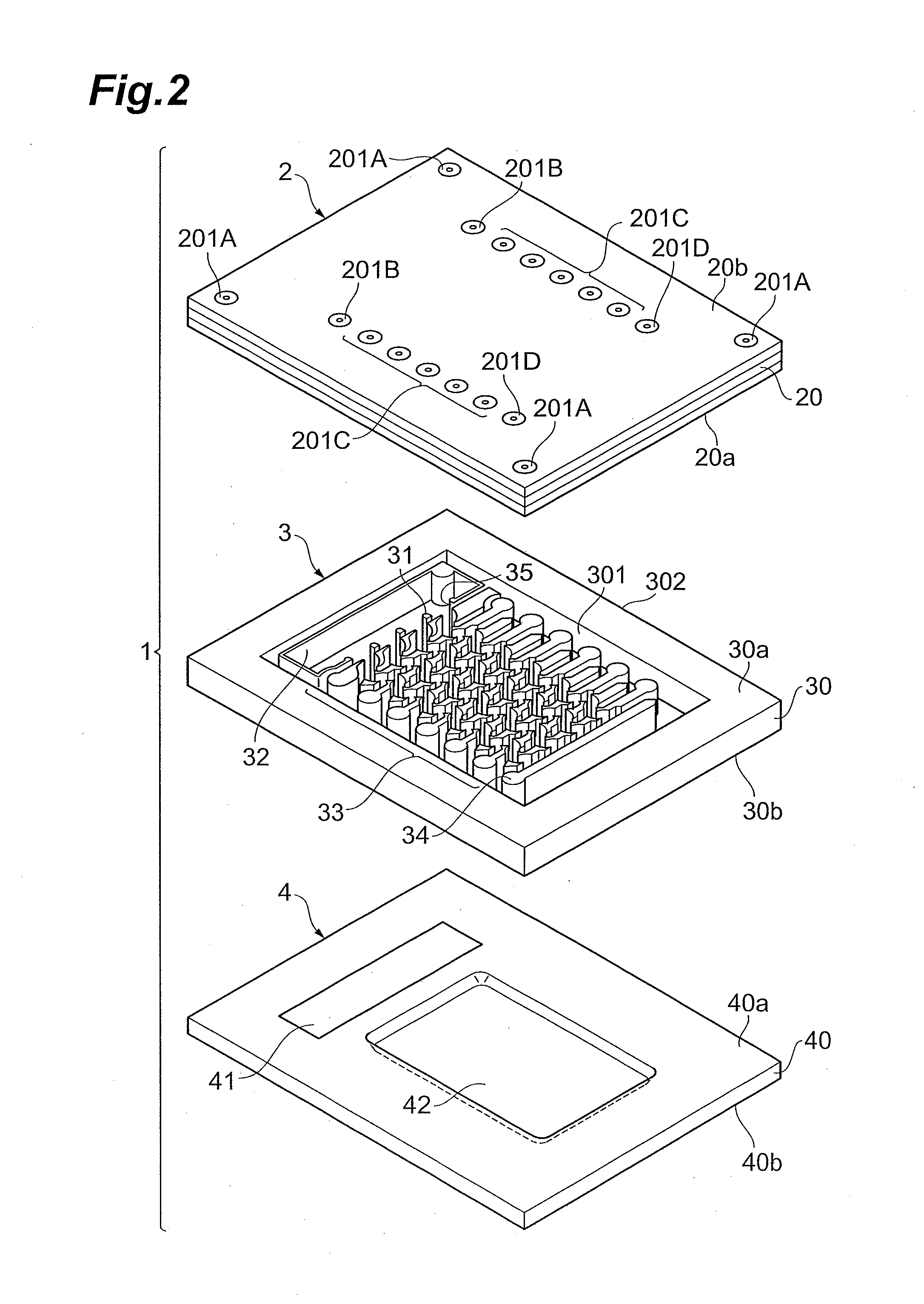
[0027]FIG. 1 is a perspective view which shows a photomultiplier tube 1 related to one preferred embodiment of the present invention. FIG. 2 is an exploded perspective view which shows the photomultiplier tube 1 shown in FIG. 1.

[0028]The photomultiplier tube 1 shown in FIG. 1 is a photomultiplier tube having a transmission-type photocathode and provided with a casing 5, that is, a housing constituted with an upper frame (a second substrate) 2, a side wall frame 3, and a lower frame (a first substrate) 4 which opposes the upper frame 2, with the side wall frame 3 kept therebetween. The photomultiplier tube 1 is an electron tube such that when light is made incident from a d...


PUM


Abstract

The photomultiplier tube 1 is provided with a casing 5 made of an upper frame 2 and a lower frame 4, an electron multiplying part 33 having dynodes 33a to 33l arrayed on the lower frame 4, a photocathode 41, and an anode part 34. Conductive layers 202 are installed on an opposing surface 20a of the upper frame 2. The electron multiplying part 33 is provided with base parts 52a to 52d of the respective dynodes 33a to 33d installed on the side of the lower frame 4, and power supplying parts 53a to 53d connected to the conductive layers 202 at one end parts of the respective base parts 52a to 52d in a direction along the opposing surface 40a. The base parts 52a to 52d are constituted in such a manner that the both end parts are joined to the opposing surface 40a, the central part is spaced away from the opposing surface 40a, and a cross sectional area at the one end part on the side of each of the power supplying parts 53a to 53d is made greater than a cross sectional area at another end part.

Description

BACKGROUND OF THE INVENTION[0001]1. Field of the Invention[0002]The present invention relates to a photomultiplier tube for detecting incident light from outside.[0003]2. Related Background Art[0004]Conventionally, compact photomultiplier tubes by utilization of fine processing technology have been developed. For example, a flat surface-type photomultiplier tube which is arranged with a photocathode, dynodes and an anode on a translucent insulating substrate is known (refer to Patent Document 1 given below). The above-described structure makes it possible to detect weak light and also downsize a device.[0005]Patent Document 1: U.S. Pat. No. 5,264,693SUMMARY OF THE INVENTION[0006]However, in the above-described conventional photomultiplier tube, since structures different in potential are arranged in close proximity to each other on an insulating substrate, there is found a decrease in withstand voltage between the structures when the photomultiplier tube is downsized, and this is a ...

Claims


Application Information

Patent Timeline
IPC IPC(8): H01J43/18
CPCH01J43/28H01J43/22
Inventor SHIMOI, HIDEKIKYUSHIMA, HIROYUKI
Owner HAMAMATSU PHOTONICS KK
Why Eureka
Try Eureka