Acoustic wave device

a technology of acoustic waves and filters, applied in the field of acoustic waves devices, can solve the problems of reducing the acoustic impedance of increasing the loss resulting from the decoupler film itself, and not being able to convert unbalanced signals to balanced signals and the revers

Active Publication Date: 2012-05-03
TAIYO YUDEN KK
View PDF14 Cites 27 Cited by
  • Summary
  • Abstract
  • Description
  • Claims
  • Application Information

AI Technical Summary

Benefits of technology

[0006]According to an aspect of the present invention, there is provided an acoustic wave device including: a first piezoelectric thin film resonator including a first lower electrode, a first upper electrode and a first piezoelectric film sandwiched between the first lower and upper electrodes, a decoupler film provided on the first upper electrode; and a second piezoelectric thi

Problems solved by technology

However, the filter using FBAR or SMR is not capable of converting unbalanced signals to balanced signals and the reverse.
Howeve

Method used


Image

  • Acoustic wave device
  • Acoustic wave device
  • Acoustic wave device

Examples


embodiment 1

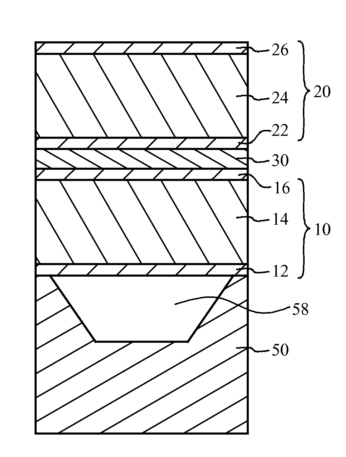
[0049]An embodiment 1 improves the piezoelectric constant of a piezoelectric film. First, a description will be given of the significance of improving the piezoelectric constant of the piezoelectric film. A structure of each film used in simulation is the same as one of the comparative example 1. The decoupler film 30 is a silicon oxide film and has an acoustic impedance of 12.7 Mrayl.

[0050]FIG. 10A is a graph of an impedance vs. frequency characteristic of the comparative example 1 in which the decoupler film 30 is a silicon oxide film. The spacing between the two modes is set to the spacing Δf between resonance frequencies. FIG. 10B is a graph of the resonance frequency spacing ratio ((fsr−far) / (fsr+far)×2×100) associated with variations of the dielectric constant (white circle), the elastic constant (black circle), and the piezoelectric constant (white triangle) of the piezoelectric films 14 and 24. The variations are values normalized by using, as reference values, the standard ...

embodiment 2

[0064]An embodiment 2 has an exemplary structure in which the electrodes have different film thicknesses. FIG. 15 illustrates a structure of a CRF according to the embodiment 2 in simulation. As illustrated in FIG. 15, T1 indicates the film thickness of each of the first lower electrode 12 and the second upper electrode 26, and T2 indicates the film thickness of each of the first upper electrode 16 and the second lower electrode 22. The other arrangements are the same as those illustrated in FIG. 1, and a description thereof is omitted here. The simulation is performed under the following conditions. Each of the first lower electrode 12, the first upper electrode 16, the second lower electrode 22, and the second upper electrode 26 is a Ru film. Each of the first piezoelectric film 14 and the second piezoelectric film 24 is an AIN film having a thickness of 800 nm and a piezoelectric constant (e33) of 1.55 C / m2. The decoupler film 30 is a silicon oxide film that is 450 nm thick. In t...

embodiment 3

[0069]An embodiment 3 has an exemplary structure in which the electrodes have different acoustic impedances. The simulation is performed by using a CRF having the same structure as one illustrated in FIG. 6 under the following conditions. The first lower electrode 12, the first upper electrode 16, the second lower electrode 22, and the second upper electrode 26 are made of Ru and are 100 nm thick. Each of the first piezoelectric film 14 and the second piezoelectric film 24 is an AIN film having a thickness of 800 nm and a piezoelectric constant (e33) equal to 1.5 times 1.55 C / m2. The decoupler film 30 is a silicon oxide film having a thickness of 450 nm. In the simulation, the acoustic impedances of the first lower electrode 12, the first upper electrode 16, the second lower electrode 22, and the second upper electrode 26 are changed. Since changing the acoustic impedances varies the frequencies, a thickness correction is made by multiplying the film thickness of each layer by an id...


PUM


Abstract

An acoustic wave device includes: a first piezoelectric thin film resonator including a first lower electrode, a first upper electrode and a first piezoelectric film sandwiched between the first lower and upper electrodes; a decoupler film provided on the first upper electrode; and a second piezoelectric thin film resonator provided on the decoupler film and including a second lower electrode, a second upper electrode and a second piezoelectric film sandwiched between the second lower and upper electrodes, wherein the first piezoelectric film and the second piezoelectric film comprise aluminum nitride and include an element increasing a piezoelectric constant of the aluminum nitride.

Description

CROSS-REFERENCE TO RELATED APPLICATION[0001]This application is based upon and claims the benefit of priority of the prior Japanese Patent Application No. 2010-245452, filed on Nov. 1, 2010, the entire contents of which are incorporated herein by reference.FIELD[0002]A certain aspect of the present invention relates to acoustic wave devices.BACKGROUND[0003]A piezoelectric thin film resonator is used as a high frequency circuit of a cellular phone or the like. There are a film bulk acoustic resonator (FBAR) type and a solidly mounted resonator (SMR) type of piezoelectric thin film resonators. In late years, the balanced output is frequently requested at a reception terminal of an antenna duplexer. However, the filter using FBAR or SMR is not capable of converting unbalanced signals to balanced signals and the reverse. Thus, there has been developed a coupled resonator filter (CRF) structure capable of converting the unbalanced signals to the balanced signals and the reverse (for exam...

Claims


Application Information

Patent Timeline
IPC IPC(8): H01L41/083H01L41/09H01L41/18H01L41/29H01L41/39H03H9/17H03H9/54
CPCH03H9/584H03H9/587H03H9/589
Inventor NISHIHARA, TOKIHIROTANIGUCHI, SHINJIYOKOYAMA, TSUYOSHISAKASHITA, TAKESHI
Owner TAIYO YUDEN KK
Why Eureka
Try Eureka