
Borderless contact for replacement gate employing selective deposition

Active Publication Date: 2012-05-24
AURIGA INNOVATIONS INC
View PDF5 Cites 57 Cited by
  • Summary
  • Abstract
  • Description
  • Claims
  • Application Information

AI Technical Summary

Benefits of technology

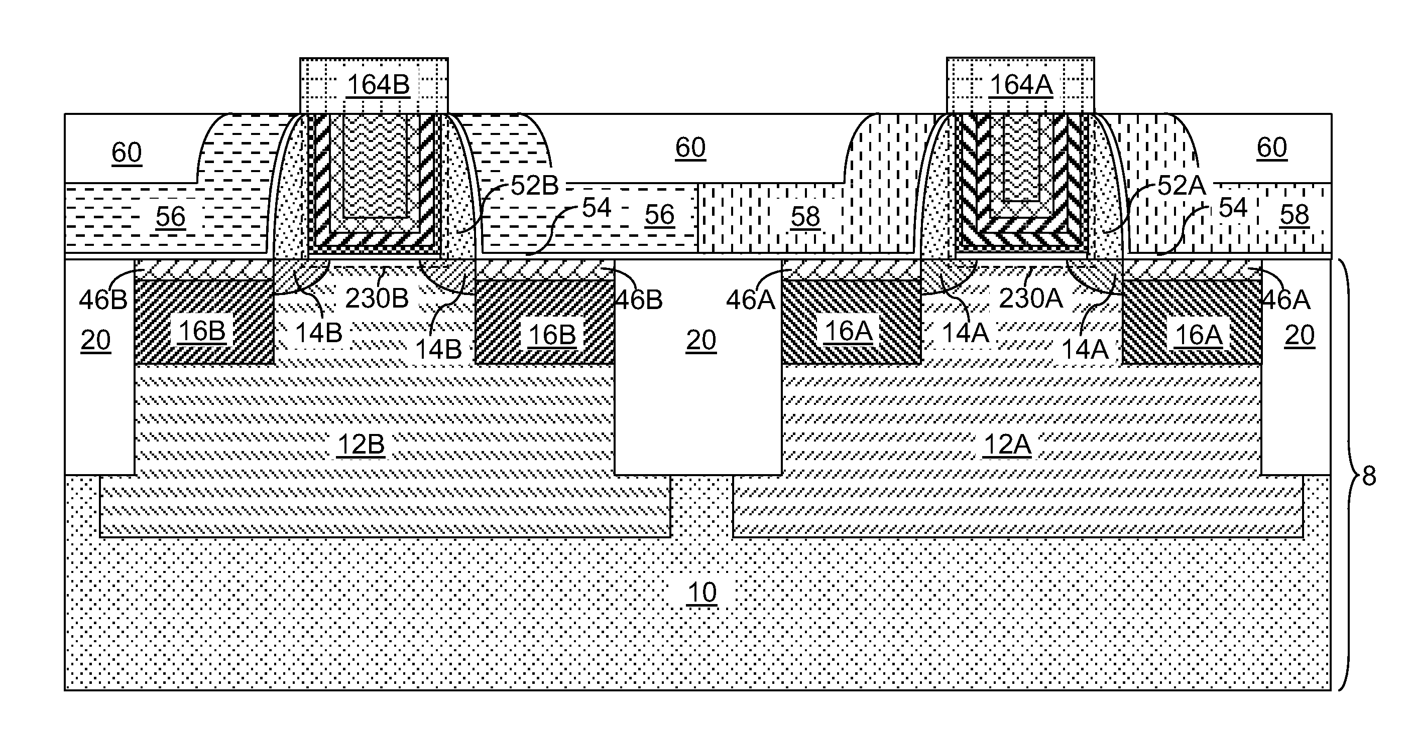
[0004]A self-aligned gate cap dielectric can be employed to form a self-aligned contact to a diffusion region of a semiconductor device, while preventing electrical short with a gate conductor due to overlay variations. In one embodiment, an electroplatable or electrolessly platable metal is selectively deposited on conductive materials in a gate electrode, for example, by electroplating or electroless plating, while the metal is not deposited on dielectric surfaces. The metal portion on top of the gate electrode is converted into a gate cap dielectric including the metal and oxygen, for example, by anodization or oxidation. In another embodiment, a self-assembling monolayer is formed on dielectric surfaces, while exposing metallic top surfaces of a gate electrode. A gate cap dielectric including a dielectric oxide is formed, for example, by atomic layer deposition (ALD) on areas not covered by the self-assembling monolayer. The self-assembling monolayer is subsequently removed. After formation of the gate cap dielectric, a contact-level dielectric layer is deposited over the gate cap dielectric, and at least one via hole is formed around the gate electrode. The gate cap dielectric functions as an etch-stop structure during formation of the via hole, so that a contact via structure formed therein is self-aligned away from the gate electrode, preventing electrical short to the gate electrode.

Problems solved by technology

As semiconductor devices shrink in each generation of semiconductor technology, formation of contact structures to source and drain regions of a field effect transistor become challenging because such contact structures not only need to provide reliable electrical contact to the source and drain regions, but also need to avoid electrically shorting to other components such as the gate electrode of the field effect transistor.

Method used


Image

  • Borderless contact for replacement gate employing selective deposition
  • Borderless contact for replacement gate employing selective deposition
  • Borderless contact for replacement gate employing selective deposition

Examples


first embodiment

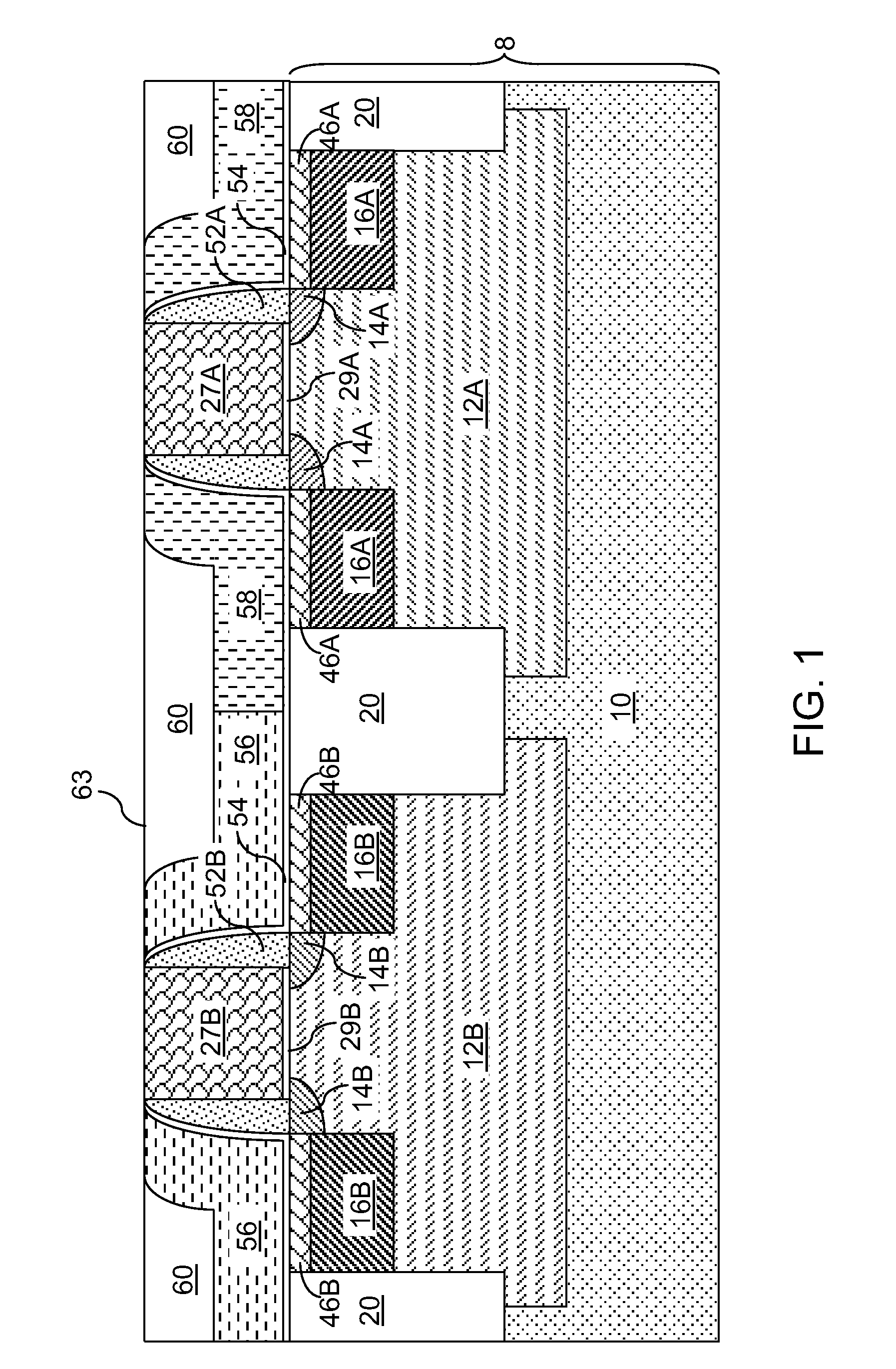
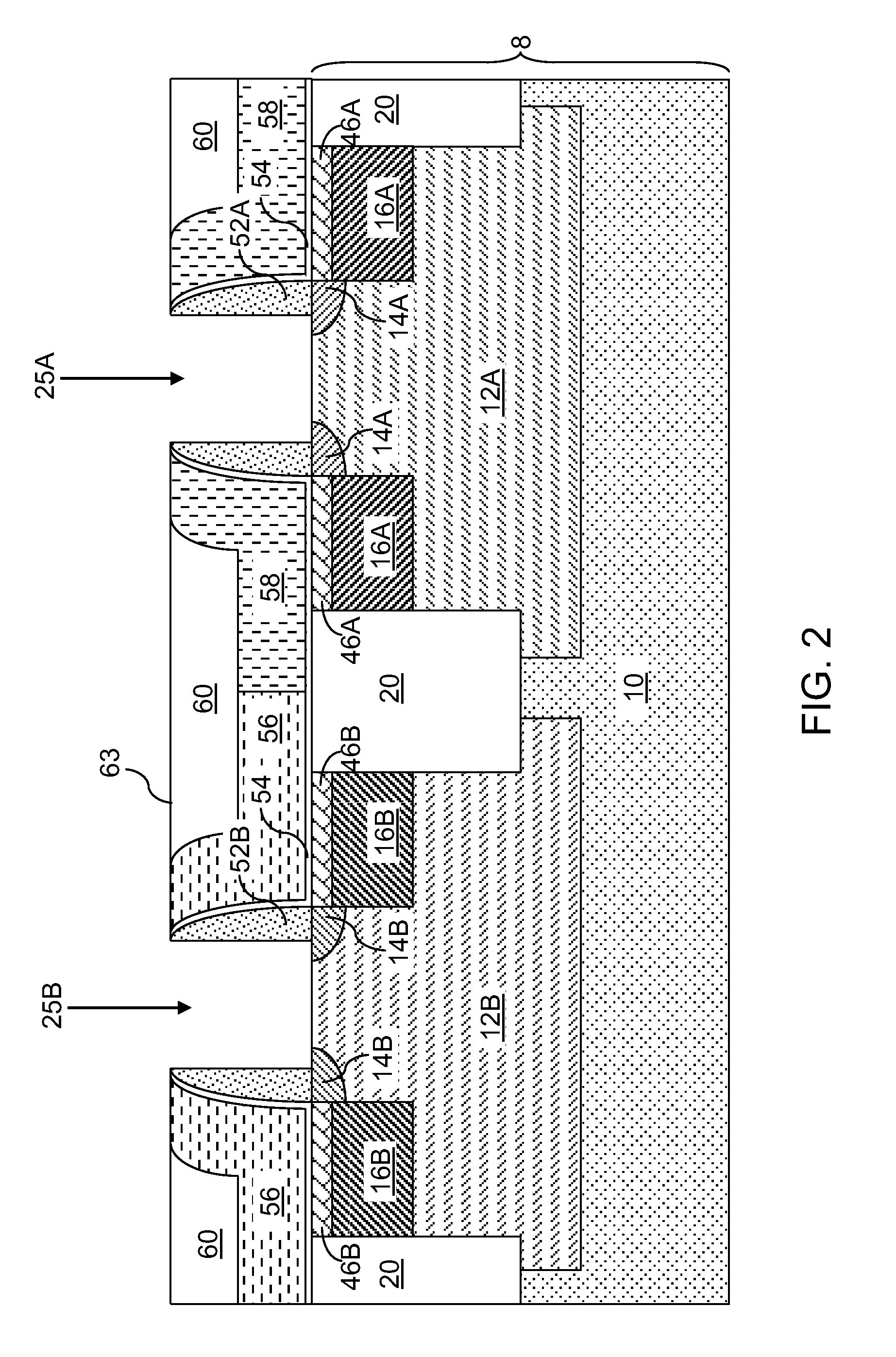
[0026]Referring to FIG. 1, a first exemplary semiconductor structure according to the present disclosure includes a semiconductor substrate 8, on which various components of field effect transistors are formed. The semiconductor substrate 8 can be a bulk substrate including a bulk semiconductor material throughout, or a semiconductor-on-insulator (SOI) substrate (not shown) containing a top semiconductor layer, a buried insulator layer located under the top semiconductor layer, and a bottom semiconductor layer located under the buried insulator layer.

[0027]Various portions of the semiconductor material in the semiconductor substrate 8 can be doped with electrical dopants of p-type or n-type at different dopant concentration levels. For example, the semiconductor substrate 8 may include an underlying semiconductor layer 10, a first conductivity type well 12B, and a second-conductivity type well 12A. The first conductivity type well 12B is doped with electrical dopants of a first cond...

second embodiment

[0074]Referring to FIG. 12, a second exemplary structure according to the present disclosure is derived from the first exemplary structure of FIG. 7 by forming a self-assembling monolayer 110. The self-assembling monolayer 110 is a monolayer of molecules that are selectively adsorbed on the dielectric surfaces of the planarization dielectric layer 60 and / or the stress-generating liners (56, 58), if present, while not adsorbing on any metallic surfaces such as the top surfaces of the gate electrodes.

[0075]The self-assembling monolayer 110 can be a polymer that selectively adsorbs to dielectric surfaces, while not adsorbing to non-dielectric surfaces. The dielectric surfaces and non-dielectric surfaces can be distinguished as hydrogen-terminated surfaces to which molecules of the self-assembling monolayer 110 do not attach and hydroxo-terminated surfaces to which molecules of the self-assembling monolayer 110 are attached. The top surface of the second exemplary structure Examples of ...


PUM


Abstract

A self-aligned gate cap dielectric can be employed to form a self-aligned contact to a diffusion region, while preventing electrical short with a gate conductor due to overlay variations. In one embodiment, an electroplatable or electrolessly platable metal is selectively deposited on conductive materials in a gate electrode, while the metal is not deposited on dielectric surfaces. The metal portion on top of the gate electrode is converted into a gate cap dielectric including the metal and oxygen. In another embodiment, a self-assembling monolayer is formed on dielectric surfaces, while exposing metallic top surfaces of a gate electrode. A gate cap dielectric including a dielectric oxide is formed on areas not covered by the self-assembling monolayer. The gate cap dielectric functions as an etch-stop structure during formation of a via hole, so that electrical shorting between a contact via structure formed therein and the gate electrode is avoided.

Description

BACKGROUND[0001]The present disclosure relates to semiconductor structures, and particularly to a metal-oxide-semiconductor field effect transistor (MOSFET) having a self-aligned dielectric gate cap and methods of manufacturing the same.[0002]As semiconductor devices shrink in each generation of semiconductor technology, formation of contact structures to source and drain regions of a field effect transistor become challenging because such contact structures not only need to provide reliable electrical contact to the source and drain regions, but also need to avoid electrically shorting to other components such as the gate electrode of the field effect transistor. Since the etch chemistry employed for the anisotropic etch process remains the same while the lateral dimension of the dielectric gate spacer shrinks with the scaling of semiconductor devices, the likelihood of overlay variations during lithographic processes causing formation of contact structures that electrically short ...

Claims


Application Information

Patent Timeline
IPC IPC(8): H01L21/28H01L29/78
CPCH01L21/823807H01L21/823842H01L21/823871H01L29/165H01L29/4966H01L29/517H01L29/7848H01L29/665H01L29/66545H01L29/6659H01L29/66636H01L29/7833H01L29/7843H01L29/518H01L21/76897H01L21/76834
Inventor EDGE, LISA F.HARAN, BALASUBRAMANIAN S.
Owner AURIGA INNOVATIONS INC
Learn More