Soldering connecting pin, semiconductor package substrate and method of mounting semiconductor chip using the same

a technology of connecting pins and semiconductor packages, which is applied in the direction of semiconductor/solid-state device details, conductors, conductive pattern formation, etc., can solve the problems of solder failure, semiconductor package substrate instability, and deformation of the completed semiconductor package substrate, so as to improve the stability of the semiconductor package substrate, reduce thermal stress, and prevent fatigue failure

Inactive Publication Date: 2012-05-24
SAMSUNG ELECTRO MECHANICS CO LTD
View PDF0 Cites 19 Cited by
  • Summary
  • Abstract
  • Description
  • Claims
  • Application Information

AI Technical Summary

Benefits of technology

[0010]The present invention has been made in an effort to provide a soldering connecting pin that includes a pin head having a hole formed therein; and a plurality of pin bodies formed on a lower surface of the pin head, wherein the pin body includes a support extended downward from the pin head and a bonding portion extended to be bent from the support, used for mounting a semiconductor chip on a printed circuit board to reduce thermal stress and prevent fatigue failure due to external shocks, thereby improving the stability of a semiconductor package substrate.

Problems solved by technology

The thermal stress has caused problems such as deformation of the completed semiconductor package substrate and failure of the solder 130 connecting the semiconductor chip 200 to the printed circuit board 100.
In addition, in the structure according to the prior art bonding the external lead 210 of the semiconductor chip 200 to the printed circuit board 100 by filling the through-hole 120 with the solder 130, when a continuous external shock is applied thereto, there was a considerable risk of fatigue failure, thereby causing instability of the semiconductor package substrate.

Method used


Image

  • Soldering connecting pin, semiconductor package substrate and method of mounting semiconductor chip using the same
  • Soldering connecting pin, semiconductor package substrate and method of mounting semiconductor chip using the same
  • Soldering connecting pin, semiconductor package substrate and method of mounting semiconductor chip using the same

Examples


Embodiment Construction

[0031]The terms and words used in the present specification and claims should not be interpreted as being limited to typical meanings or dictionary definitions, but should be interpreted as having meanings and concepts relevant to the technical scope of the present invention based on the rule according to which an inventor can appropriately define the concept of the term to describe most appropriately the best method he or she knows for carrying out the invention.

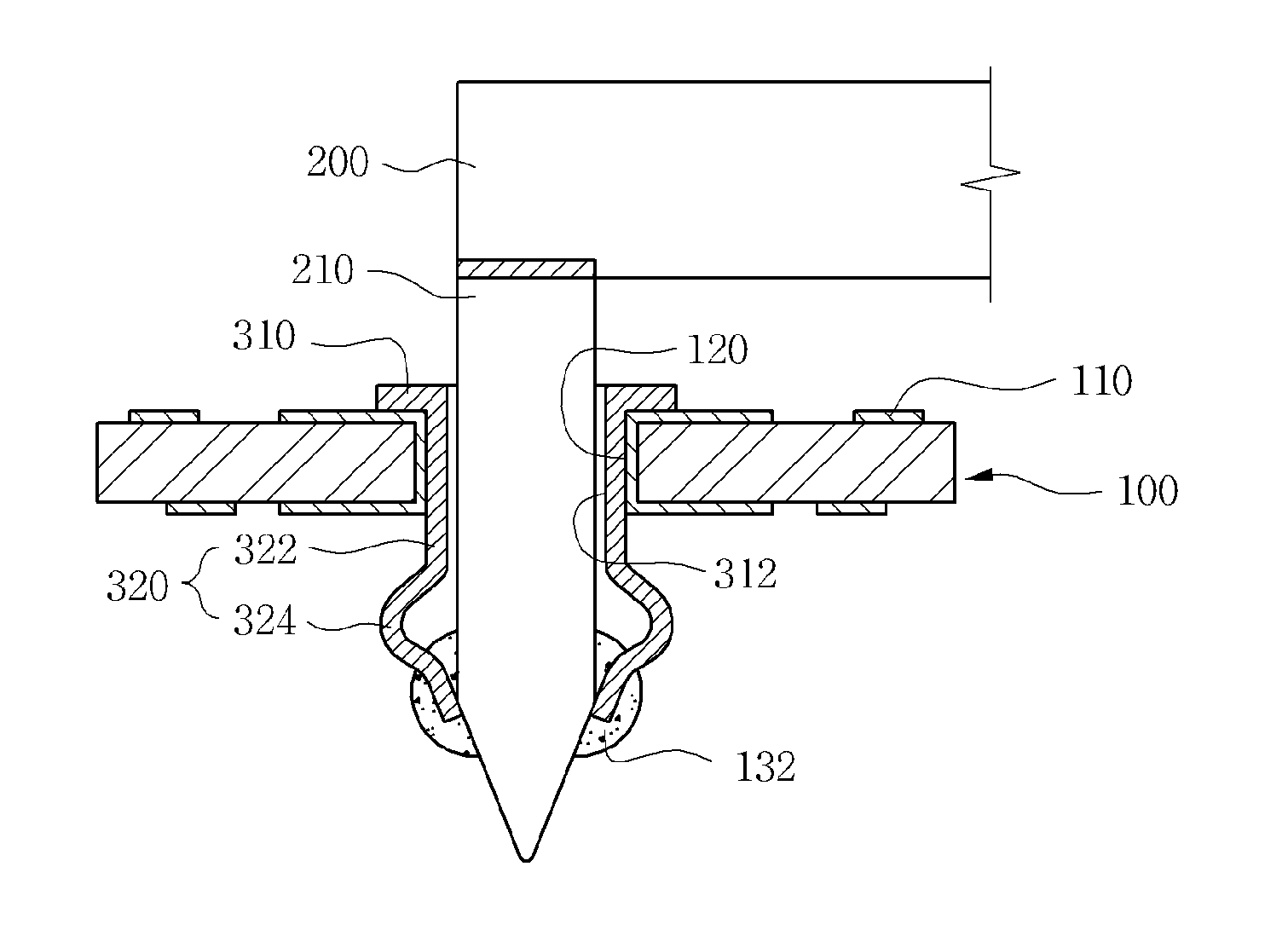
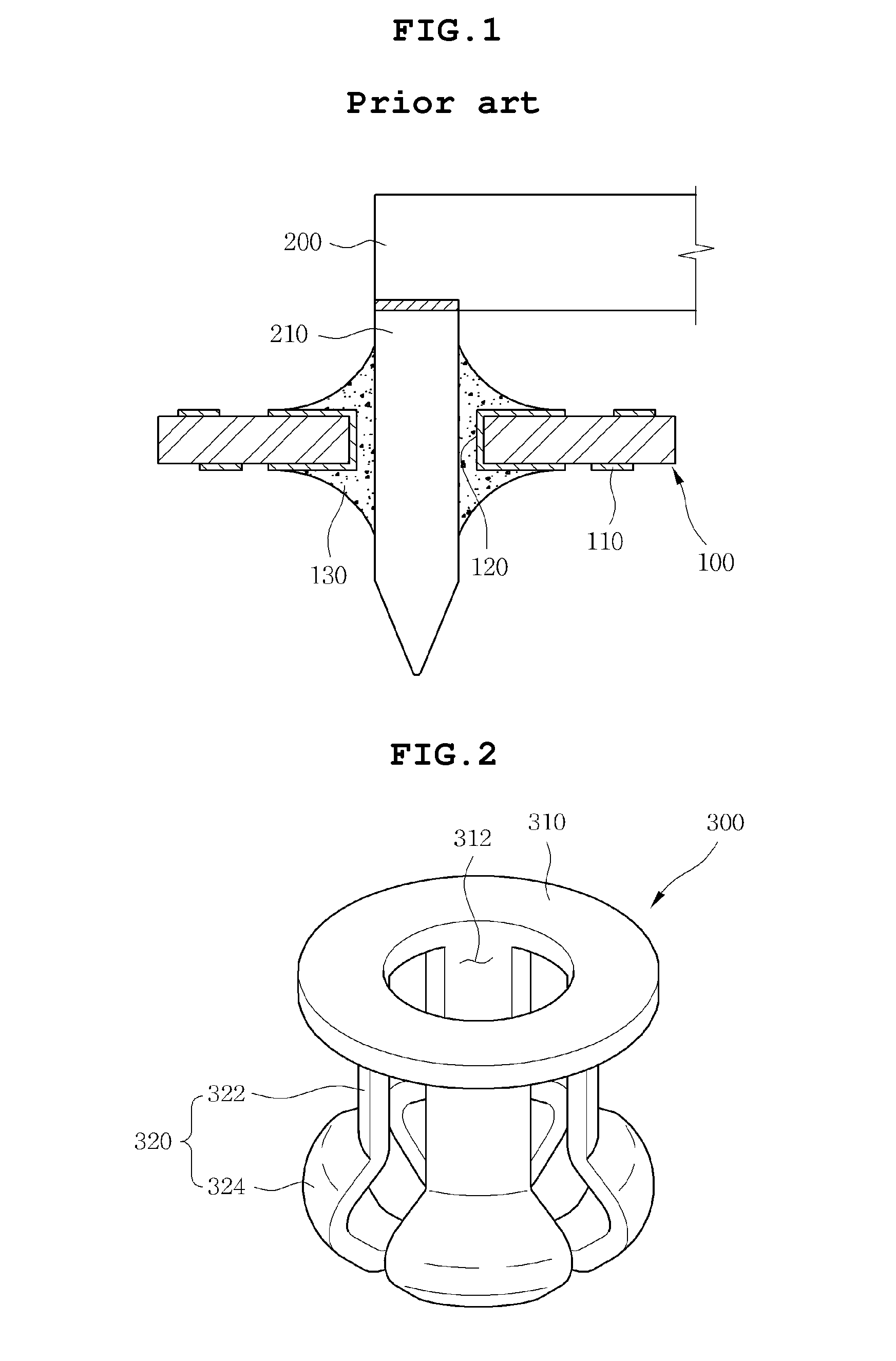
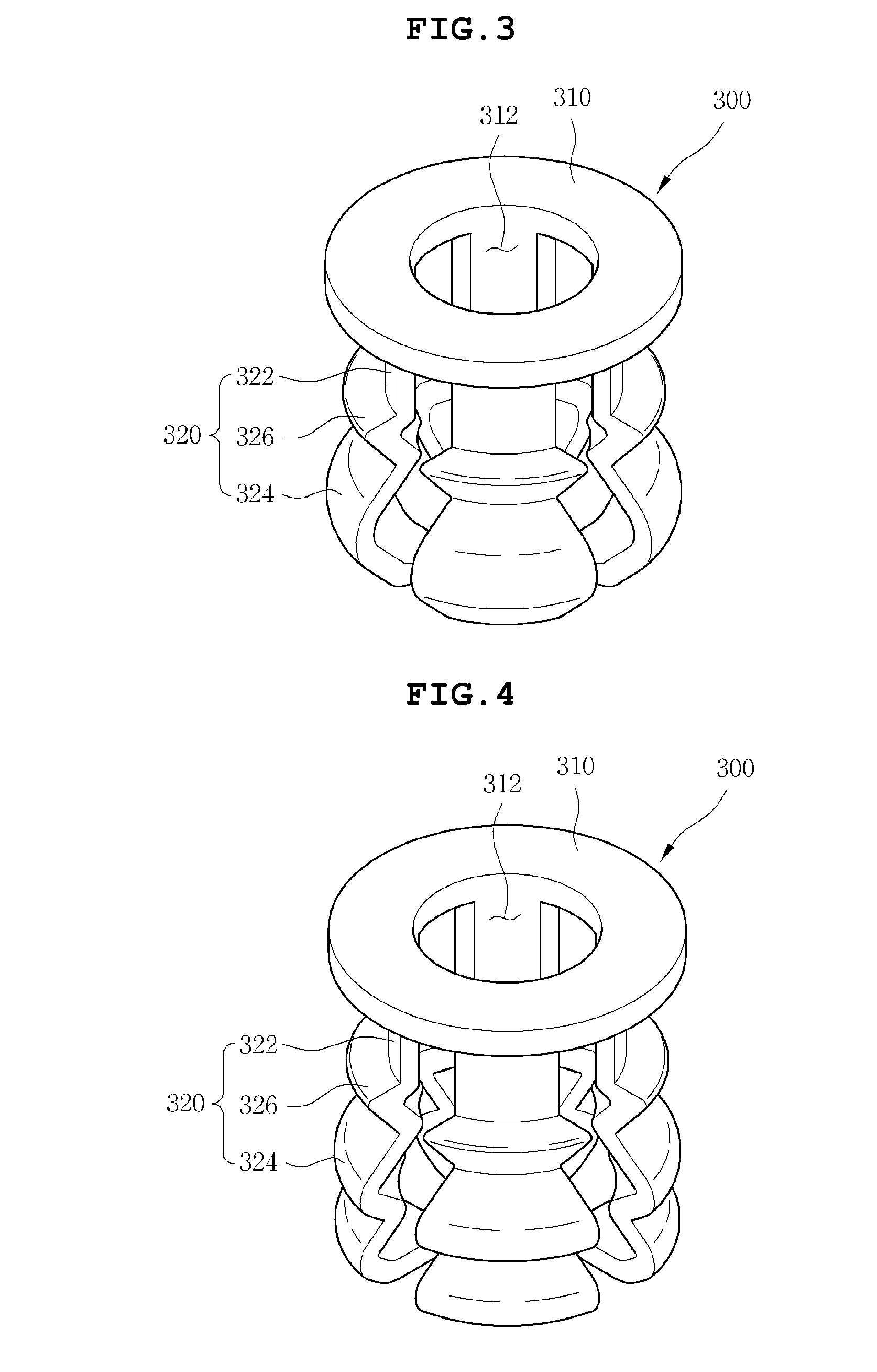
[0032]The above and other objects, features and advantages of the present invention will be more clearly understood from the following detailed description taken in conjunction with the accompanying drawings. In the specification, in adding reference numerals to components throughout the drawings, it is to be noted that like reference numerals designate like components even though components are shown in different drawings. Further, when it is determined that the detailed description of the known art related to the present ...


PUM

PropertyMeasurementUnit
circumferenceaaaaaaaaaa
shapeaaaaaaaaaa
lengthaaaaaaaaaa

Abstract

Disclosed herein are a soldering connecting pin, a semiconductor package substrate and a method of mounting a semiconductor chip using the same. A semiconductor chip is mounted on the printed circuit board using the soldering connecting pin inserted into a through-hole of the printed circuit board, thereby preventing deformation of the semiconductor package substrate and fatigue failure due to external shocks.

Description

CROSS REFERENCE TO RELATED APPLICATION[0001]This application claims the benefit of Korean Patent Application No. 10-2010-0117694, filed on Nov. 24, 2010, entitled “Soldering Connecting Pin, Semiconductor Package Substrate and Method of Mounting Semiconductor Chip Using the Same”, which is hereby incorporated by reference in its entirety into this application.BACKGROUND OF THE INVENTION[0002]1. Technical Field[0003]The present invention relates to a soldering connecting pin, a semiconductor package substrate and a method of mounting a semiconductor chip using the same.[0004]2. Description of the Related Art[0005]In accordance with the recent trend of compactness and slimness of electronic devices, the demand for mounting technologies using a semiconductor package substrate on which components may be mounted, at high density, with high accuracy, and with high integration has increased. In accordance with the trend of high-density, high-accuracy, and high-integration of the components,...

Claims


Application Information

Patent Timeline
Patent Type & Authority Applications(United States)
IPC IPC(8): H01R9/00H05K3/00H01B5/00
CPCH01L2924/01082Y10T29/49155H05K3/3447H05K2201/10166H05K2201/10401H05K3/306H01L2924/1305H01L2924/13055H01L2924/014H01L2924/0105H01L2924/01047H01L2924/01033H01L2924/01006H01L2924/01005H01L2924/0103H01L2924/01029H01L2224/81986H01L2224/81951H01L2224/8192H01L2224/81906H01L2224/81899H01L2224/81815H01L24/13H01L24/16H01L24/81H01L2224/13017H01L2224/1601H01L2224/16057H01L2224/16058H01L2224/16059H01L2224/1607H01L2224/16235H01L2224/16501H01L2224/811H01L2224/81193H01L2224/81385H01L2224/81447H01L2924/00014H01L2924/00H01L2924/351H01L23/488H01L23/49811
Inventor RYU, JI MANLEE, KWAN HOHAN, KYU BUMCHOI, SEOG MOONKIM, JIN SU
Owner SAMSUNG ELECTRO MECHANICS CO LTD
Why Eureka
Try Eureka