Nano-optic filter array based sensor

a filter array and sensor technology, applied in the field of nano-optic filter array based sensor, can solve the problems of resolution degradation, limited adoption of this technology, and limited application to centralized labs with scaled testing protocols, etc., and achieve the effect of improving the miniaturization of spectral sensing

Active Publication Date: 2012-05-24
NANOLAMBDA
View PDF1 Cites 111 Cited by
  • Summary
  • Abstract
  • Description
  • Claims
  • Application Information

AI Technical Summary

Problems solved by technology

The challenge is that the adoption of this technology has been limited due to the size of the equipment and the associated cost.
Therefore, its application has often been limited to centralized labs with scaled testing protocols.
One of the issues encountered when trying to miniaturize the spectrometer is the resolution degradation.
The shorter the distances, the higher the resolution degradation will be.
However, there is a certain limitation to how narrow the bandwidths of the filters can be, especially when these filters are fabricated in an array configuration.
There are some other issues in using these optical spectroscopy technologies.
In these systems, individual variation in skin or nail properties and in blood vessel placement can significantly affect the accuracy of the measurements.

Method used


Image

  • Nano-optic filter array based sensor
  • Nano-optic filter array based sensor
  • Nano-optic filter array based sensor

Examples


Embodiment Construction

[0049]Unless otherwise specified, the words “a” or “an” as used herein mean “one or more”. The term “light” includes visible light as well as UV and IR radiation.

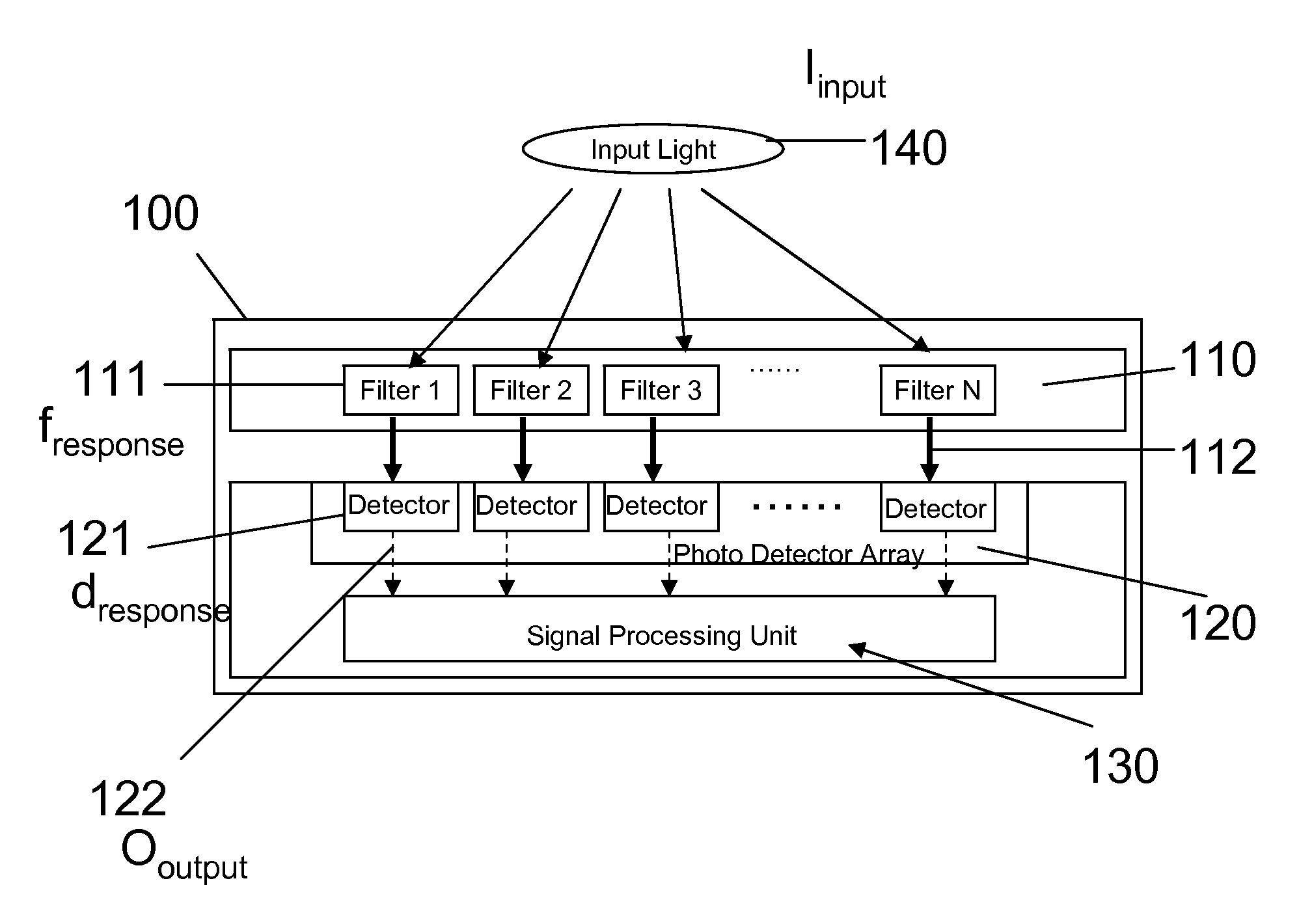
[0050]In FIG. 1, a digital filter spectrum sensor 100 is shown containing a set of filters 110, a set or array of detectors 120 (such as a photo diode array or another suitable photodetector array), and a signal processing unit 130. The filters can be made of dielectric or metallic materials, can be waveguide structures, grating structures, Fabry-Perot etalon structures, or plasmonic filter structures.

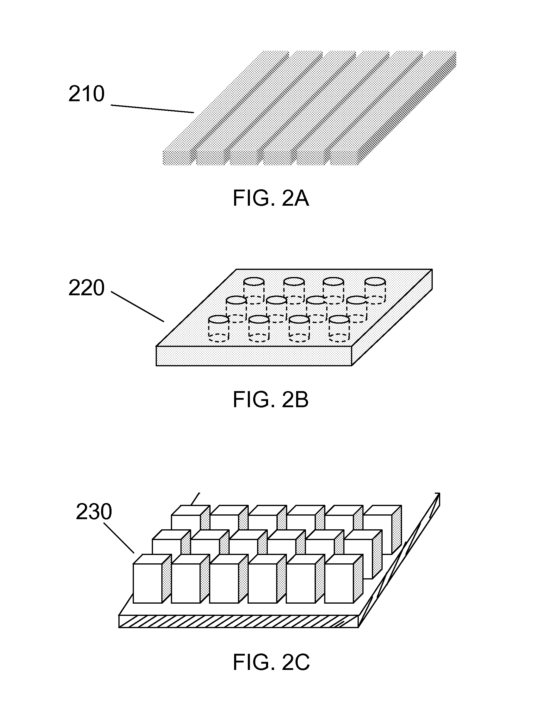
[0051]The examples of plasmonic filter structures are shown in FIGS. 2A, 2B, and 2C. In FIG. 2A, the plasmonic filter device 210 shows the metallic nanowire or island structure. In FIG. 2B, the plasmonic filter device 220 shows the metallic film with apertures or holes. Examples of such devices 210 and 220 are described for example in U.S. Patent Application Pub. No. 2006 / 0273245 A1, the disclosure of which is hereby incorpora...


PUM

PropertyMeasurementUnit
sizesaaaaaaaaaa
transmittanceaaaaaaaaaa
reflectanceaaaaaaaaaa

Abstract

A device such as a filter or reflector includes a conductive layer including a periodic pattern of elements. The elements have shapes and sizes configured such that a transmittance or reflectance spectrum of the conductive layer has a drop at a long-wavelength end. The elements have a period configured such that the spectrum has a dip at a Plasmon mode resonant wavelength. The spectrum further includes a peal- between the dip and the drop.

Description

[0001]The present application claims priority to U.S. Provisional Patent Application Ser. No. 61 / 161,892, filed Mar. 20, 2009, the disclosure of which is hereby incorporated by reference in its entirety.BACKGROUND OF THE INVENTION[0002]Optical spectroscopy technology has been widely used to detect, quantify and analyze the characteristics or concentration of a physical, chemical or biological target object such as a blood sample. This technology can also be used in other in vivo chemometric analyses of chemical components of tissues or organs in a living organism. A variety of spectral techniques involve absorption, transmission, reflection, emission, and scattering (including elastic and non-elastic) of radiations applied to a target sample. The radiations used span over a wide range and include UV, Visual, NIR (Near Infrared), SWIR (Short-Wavelength Infrared), MWIR (Medium-Wavelength Infrared), and LWIR (Long-Wavelength Infrared) light.[0003]Optical spectroscopy is also used for h...

Claims


Application Information

Patent Timeline
Patent Type & Authority Applications(United States)
IPC IPC(8): G01J3/46G01N21/17G06F17/50G01N21/78G01J1/42B82Y15/00
CPCA61B5/0071A61B5/0075A61B5/1455A61B2562/0233A61B2562/0285A61B2562/046G02B5/204G01J3/02G01J3/0205G01J3/36G01J2003/1213G01N21/554G02B5/201B82Y20/00
Inventor CHOI, BYUNG ILLEE, BYOUNGHEESONG, MIN KYU
Owner NANOLAMBDA
Why Eureka
Try Eureka